Physics for Electronics Engineering
PH3254 - Physics II - 2nd Semester - ECE Department - 2021 Regulation

2021 regulation - 1st year, 2nd semester paper for ECE Department (Electronics and Communication Engineering Department). Subject Code: PH3254, Subject Name: Physics for Electronics Engineering, Batch: 2021, 2022, 2023, 2024. Institute: Anna University Affiliated Engineering College, TamilNadu. This page has Physics for Electronics Engineering study material, notes, semester question paper pdf download, important questions, lecture notes.
PDF Download Links
- (PH3254 2021 Regulation) Physics for Electronics Engineering: Semester Question Paper 2024 April May
- (PH3254 2021 Regulation) Physics for Electronics Engineering: Semester Question Paper 2023 Nov Dec
- (PH3254 2021 Regulation) Physics for Electronics Engineering: Semester Question Paper 2023 April May
- (PH3254 2021 Regulation) Physics for Electronics Engineering: Semester Question Paper 2022 Nov Dec
- (PH3254 2021 Regulation) Physics for Electronics Engineering: Semester Question Paper 2022 April May
- PH3254 Physics for Electronics Engineering Reg2021 Question Paper Nov Dec 2022 PDF Download
- PH3254 Physics for Electronics Engineering Reg2021 Previous Question Paper April May 2019 Reg2017 PD
- PH3254 Physics for Electronics Engineering Reg2021 Previous Question Paper April May 2018 Reg2017 PD
- PH3254 Physics for Electronics Engineering Reg2021 Question Paper April May 2022 PDF Download
- (PH3254 2021 Regulation) Physics for Electronics Engineering: Notes - Hand Writing
- (PH3254) Physics for Electronics Engineering: Hand Written Notes - Unit 5:- Nano Devices
- (PH3254) Physics for Electronics Engineering: Hand Written Notes - Unit 4:- Optical Properties of Materials
- (PH3254) Physics for Electronics Engineering: Hand Written Notes - Unit 3:- Semiconductors and Transport Physics
- (PH3254) Physics for Electronics Engineering: Hand Written Notes - Unit 2:- Electrical and Magnetic Properties of Materials
- (PH3254) Physics for Electronics Engineering: Hand Written Notes - Unit 1:- Crystallography
- PH3254 Physics for Electronics Engineering Reg2021 Notes Unit V PDF Download
- PH3254 Physics for Electronics Engineering Reg2021 Notes Unit III PDF Download
- PH3254 Physics for Electronics Engineering Reg2021 Notes Unit II PDF Download
- (PH3254 2021 Regulation) Physics for Electronics Engineering: Important Questions
- (PH3254) Physics for Electronics Engineering: Question Bank and Important 2 Marks Questions with Answer
- (PH3254) Physics for Electronics Engineering: Important Questions with Answer - Unit 5:- Nano Devices
- (PH3254) Physics for Electronics Engineering: Important Questions with Answer - Unit 4:- Optical Properties of Materials
- (PH3254) Physics for Electronics Engineering: Important Questions with Answer - Unit 3:- Semiconductors and Transport Physics
- (PH3254) Physics for Electronics Engineering: Important Questions with Answer - Unit 2:- Electrical and Magnetic Properties of Materials
Physics for Electronics Engineering
- Introduction of Crystallography
- Crystalline Materials
- Amorphous Materials
- Space Lattice (crystal Lattice)
- Basis of Crystal structure
- Unit Cell
- Lattice Parameters of the Unit Cell
- Crystal Systems
- Bravais Lattice
- Simple Cubic (SC) Structure
- Body - Centred Cubic (BCC) Structure
- Face-Centred Cubic (FCC) Structure
- Diamond Cubic (DC) Structure
- Sodium Chloride Structure
- Zinc Sulphide (ZnS) Structure
- Linear Density and Planar Density
- Directions in Crystal
- Planes in Crystals and Miller Indices
- Distance Between Successive Planes
- Example Use of Milliner Indices
- Pattern Alignment
- Imperfections or Defects in Crystals
- Anna University Solved Problems
- Important Two Marks & 16 Marks Question and Answers
- Electrical Properties of Materials
- Classical Free Electron (CFE) Theory of Metals
- Expression for Electrical Conductivity of a Metal (Derivation)
- Expression for Thermal Conductivity of a Metal (Derivation)
- Quantum Free Electron (QFE) Theory
- Degenerate States and Tunneling
- Fermi-Dirac Statistics
- Density of Energy States
- Electron in Periodic Potential
- Energy Bands in Solids
- Tight Binding Approximation
- Effective Mass of Electron and Hole
- Concept of Hole: (or) Effective or Negative Mass of Electron
- Anna University Solved Problems in Electrical Properties of Materials
- Important Two Marks Question and Answers in Electrical Properties of Materials
- 16 marks Important Questions and Assignment Problems
- Introduction of Magnetic Properties of Materials
- Classification of Magnetic Materials
- Paramagnetism in the Conduction Electrons in Metals
- Ferromagnetic Effect
- Quantum Interference Effect
- Quantum Interference Devices
- Giant Magneto Resistance (GMR) - Devices Sensor - Spin Valve
- Anna University Solved Problems in Magnetic Properties of Materials
- Two Mark Questions & Answers and 16 Mark Questions in Magnetic Properties of Materials
- Semiconductors
- Direct and Indirect Band Gap Semiconductors
- Intrinsic Semiconductors and Energy Band Diagram
- Carrier Concentration in Intrinsic Semiconductors
- Density of holes in Valence Band of Intrinsic Semiconductor (Derivation)
- Intrinsic Carrier Concentration
- Extrinsic or Impure Semiconductors
- n - type Semiconductor
- Carrier Concentration in n-type Semiconductors
- p - type Semiconductor
- Concentration of Holes in Valence Band of p-type Semiconductors
- Variation of Carrier Concentration with Temperature and Impurity
- Carrier Transport in Semiconductor Mobility
- Mobility
- Drift and Diffusion Current
- Hall effect in n-type semiconductor
- Hall effect in p-type semiconductor
- Hall Devices
- Schottky Diode
- Ohmic Contacts
- Important Problems in Semiconductors and Transport Physics
- Important Questions with Answers in Semiconductors and Transport Physics
- Optical Materials
- Optical Processes in Semiconductors
- Absorption and Emission of Light in Semiconductors
- Injection and Radiative Recombination
- Carrier Generation and Recombination Processes
- Optical Absorption Loss and Gain
- Optical Processes in Quantum Wells
- Optoelectronic Devices: Light Detectors
- Solar Cell
- Light Emitting Diode
- Laser Diodes
- Organic Semiconductors: Optical Processes and Devices
- Excitonic State & Organic Light Emitting Diode (OLED)
- Electro - Optic Effects
- Non Linear Optics
- Electro Optic Modulators
- Optical (Photonic) Switching
- Plasmonics
- Important Questions with Answers in Optical Properties of Materials
- Introduction of Nano Devices
- Density of States for Solids
- Significance Between Fermi Energy and Volume of the Material
- Quantum Confinement
- Quantum Structures
- Density of States in Quantum Well, Quantum Wire and Quantum Dot Structure
- Bandgap of Nanomaterials
- Single Electron Phenomena
- Single Electron Transistor (SET)
- Conductivity of Metallic Nanowires
- Ballistic Transport
- Quantum Resistance and Conductance
- Carbon Nanotubes (CNT)
- Properties of Carbon Nanotubes (CNTs)
- Applications of Carbon Nanotubes (CNTs)
- Spintronics Devices and Applications
- Optics in Quantum Structures
- Quantum Well Laser
- Important Questions in Nano Devices
- Anna University Model Question Papers
PDF Download Links
- (PH3254 2021 Regulation) Physics for Electronics Engineering: Semester Question Paper 2024 April May
- (PH3254 2021 Regulation) Physics for Electronics Engineering: Semester Question Paper 2023 Nov Dec
- (PH3254 2021 Regulation) Physics for Electronics Engineering: Semester Question Paper 2023 April May
- (PH3254 2021 Regulation) Physics for Electronics Engineering: Semester Question Paper 2022 Nov Dec
- (PH3254 2021 Regulation) Physics for Electronics Engineering: Semester Question Paper 2022 April May
- PH3254 Physics for Electronics Engineering Reg2021 Question Paper Nov Dec 2022 PDF Download
- PH3254 Physics for Electronics Engineering Reg2021 Previous Question Paper April May 2019 Reg2017 PD
- PH3254 Physics for Electronics Engineering Reg2021 Previous Question Paper April May 2018 Reg2017 PD
- PH3254 Physics for Electronics Engineering Reg2021 Question Paper April May 2022 PDF Download
- (PH3254 2021 Regulation) Physics for Electronics Engineering: Notes - Hand Writing
- (PH3254) Physics for Electronics Engineering: Hand Written Notes - Unit 5:- Nano Devices
- (PH3254) Physics for Electronics Engineering: Hand Written Notes - Unit 4:- Optical Properties of Materials
- (PH3254) Physics for Electronics Engineering: Hand Written Notes - Unit 3:- Semiconductors and Transport Physics
- (PH3254) Physics for Electronics Engineering: Hand Written Notes - Unit 2:- Electrical and Magnetic Properties of Materials
- (PH3254) Physics for Electronics Engineering: Hand Written Notes - Unit 1:- Crystallography
- PH3254 Physics for Electronics Engineering Reg2021 Notes Unit V PDF Download
- PH3254 Physics for Electronics Engineering Reg2021 Notes Unit III PDF Download
- PH3254 Physics for Electronics Engineering Reg2021 Notes Unit II PDF Download
- (PH3254 2021 Regulation) Physics for Electronics Engineering: Important Questions
- (PH3254) Physics for Electronics Engineering: Question Bank and Important 2 Marks Questions with Answer
- (PH3254) Physics for Electronics Engineering: Important Questions with Answer - Unit 5:- Nano Devices
- (PH3254) Physics for Electronics Engineering: Important Questions with Answer - Unit 4:- Optical Properties of Materials
- (PH3254) Physics for Electronics Engineering: Important Questions with Answer - Unit 3:- Semiconductors and Transport Physics
- (PH3254) Physics for Electronics Engineering: Important Questions with Answer - Unit 2:- Electrical and Magnetic Properties of Materials
Physics for Electronics Engineering
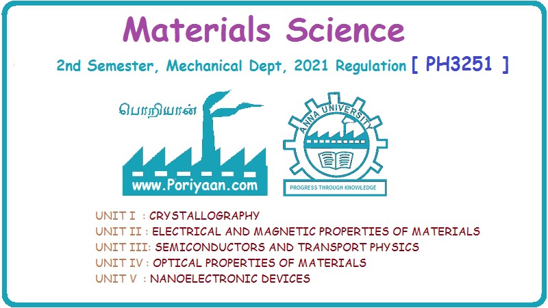
Unit I: Crystallography
- Introduction of Crystallography
- Crystalline Materials
- Amorphous Materials
- Space Lattice (crystal Lattice)
- Basis of Crystal structure
- Unit Cell
- Lattice Parameters of the Unit Cell
- Crystal Systems
- Bravais Lattice
- Simple Cubic (SC) Structure
- Body - Centred Cubic (BCC) Structure
- Face-Centred Cubic (FCC) Structure
- Diamond Cubic (DC) Structure
- Sodium Chloride Structure
- Zinc Sulphide (ZnS) Structure
- Linear Density and Planar Density
- Directions in Crystal
- Planes in Crystals and Miller Indices
- Distance Between Successive Planes
- Example Use of Milliner Indices
- Pattern Alignment
- Imperfections or Defects in Crystals
- Anna University Solved Problems
- Important Two Marks & 16 Marks Question and Answers
Unit II: Electrical and Magnetic Properties of Materials
- Electrical Properties of Materials
- Classical Free Electron (CFE) Theory of Metals
- Expression for Electrical Conductivity of a Metal (Derivation)
- Expression for Thermal Conductivity of a Metal (Derivation)
- Quantum Free Electron (QFE) Theory
- Degenerate States and Tunneling
- Fermi-Dirac Statistics
- Density of Energy States
- Electron in Periodic Potential
- Energy Bands in Solids
- Tight Binding Approximation
- Effective Mass of Electron and Hole
- Concept of Hole: (or) Effective or Negative Mass of Electron
- Anna University Solved Problems in Electrical Properties of Materials
- Important Two Marks Question and Answers in Electrical Properties of Materials
- 16 marks Important Questions and Assignment Problems
- Introduction of Magnetic Properties of Materials
- Classification of Magnetic Materials
- Paramagnetism in the Conduction Electrons in Metals
- Ferromagnetic Effect
- Quantum Interference Effect
- Quantum Interference Devices
- Giant Magneto Resistance (GMR) - Devices Sensor - Spin Valve
- Anna University Solved Problems in Magnetic Properties of Materials
- Two Mark Questions & Answers and 16 Mark Questions in Magnetic Properties of Materials
Unit III: Semiconductors and Transport Physics
- Semiconductors
- Direct and Indirect Band Gap Semiconductors
- Intrinsic Semiconductors and Energy Band Diagram
- Carrier Concentration in Intrinsic Semiconductors
- Density of holes in Valence Band of Intrinsic Semiconductor (Derivation)
- Intrinsic Carrier Concentration
- Extrinsic or Impure Semiconductors
- n - type Semiconductor
- Carrier Concentration in n-type Semiconductors
- p - type Semiconductor
- Concentration of Holes in Valence Band of p-type Semiconductors
- Variation of Carrier Concentration with Temperature and Impurity
- Carrier Transport in Semiconductor Mobility
- Mobility
- Drift and Diffusion Current
- Hall effect in n-type semiconductor
- Hall effect in p-type semiconductor
- Hall Devices
- Schottky Diode
- Ohmic Contacts
- Important Problems in Semiconductors and Transport Physics
- Important Questions with Answers in Semiconductors and Transport Physics
Unit IV: Optical Properties of Materials
- Optical Materials
- Optical Processes in Semiconductors
- Absorption and Emission of Light in Semiconductors
- Injection and Radiative Recombination
- Carrier Generation and Recombination Processes
- Optical Absorption Loss and Gain
- Optical Processes in Quantum Wells
- Optoelectronic Devices: Light Detectors
- Solar Cell
- Light Emitting Diode
- Laser Diodes
- Organic Semiconductors: Optical Processes and Devices
- Excitonic State & Organic Light Emitting Diode (OLED)
- Electro - Optic Effects
- Non Linear Optics
- Electro Optic Modulators
- Optical (Photonic) Switching
- Plasmonics
- Important Questions with Answers in Optical Properties of Materials
Unit V: Nano Devices
- Introduction of Nano Devices
- Density of States for Solids
- Significance Between Fermi Energy and Volume of the Material
- Quantum Confinement
- Quantum Structures
- Density of States in Quantum Well, Quantum Wire and Quantum Dot Structure
- Bandgap of Nanomaterials
- Single Electron Phenomena
- Single Electron Transistor (SET)
- Conductivity of Metallic Nanowires
- Ballistic Transport
- Quantum Resistance and Conductance
- Carbon Nanotubes (CNT)
- Properties of Carbon Nanotubes (CNTs)
- Applications of Carbon Nanotubes (CNTs)
- Spintronics Devices and Applications
- Optics in Quantum Structures
- Quantum Well Laser
- Important Questions in Nano Devices
- Anna University Model Question Papers
PDF Download Links
- (PH3254 2021 Regulation) Physics for Electronics Engineering: Semester Question Paper 2024 April May
- (PH3254 2021 Regulation) Physics for Electronics Engineering: Semester Question Paper 2023 Nov Dec
- (PH3254 2021 Regulation) Physics for Electronics Engineering: Semester Question Paper 2023 April May
- (PH3254 2021 Regulation) Physics for Electronics Engineering: Semester Question Paper 2022 Nov Dec
- (PH3254 2021 Regulation) Physics for Electronics Engineering: Semester Question Paper 2022 April May
- PH3254 Physics for Electronics Engineering Reg2021 Question Paper Nov Dec 2022 PDF Download
- PH3254 Physics for Electronics Engineering Reg2021 Previous Question Paper April May 2019 Reg2017 PD
- PH3254 Physics for Electronics Engineering Reg2021 Previous Question Paper April May 2018 Reg2017 PD
- PH3254 Physics for Electronics Engineering Reg2021 Question Paper April May 2022 PDF Download
- (PH3254 2021 Regulation) Physics for Electronics Engineering: Notes - Hand Writing
- (PH3254) Physics for Electronics Engineering: Hand Written Notes - Unit 5:- Nano Devices
- (PH3254) Physics for Electronics Engineering: Hand Written Notes - Unit 4:- Optical Properties of Materials
- (PH3254) Physics for Electronics Engineering: Hand Written Notes - Unit 3:- Semiconductors and Transport Physics
- (PH3254) Physics for Electronics Engineering: Hand Written Notes - Unit 2:- Electrical and Magnetic Properties of Materials
- (PH3254) Physics for Electronics Engineering: Hand Written Notes - Unit 1:- Crystallography
- PH3254 Physics for Electronics Engineering Reg2021 Notes Unit V PDF Download
- PH3254 Physics for Electronics Engineering Reg2021 Notes Unit III PDF Download
- PH3254 Physics for Electronics Engineering Reg2021 Notes Unit II PDF Download
- (PH3254 2021 Regulation) Physics for Electronics Engineering: Important Questions
- (PH3254) Physics for Electronics Engineering: Question Bank and Important 2 Marks Questions with Answer
- (PH3254) Physics for Electronics Engineering: Important Questions with Answer - Unit 5:- Nano Devices
- (PH3254) Physics for Electronics Engineering: Important Questions with Answer - Unit 4:- Optical Properties of Materials
- (PH3254) Physics for Electronics Engineering: Important Questions with Answer - Unit 3:- Semiconductors and Transport Physics
- (PH3254) Physics for Electronics Engineering: Important Questions with Answer - Unit 2:- Electrical and Magnetic Properties of Materials

PH3254
PHYSICS FOR ELECTRONICS
ENGINEERING
COURSE OBJECTIVES:
i. To make the students
to understand the basics of crystallography and its importance in studying materials properties.
ii. To understand the electrical properties of materials
including free electron
theory, applications of quantum mechanics and magnetic materials.
iii. To instil knowledge on physics of semiconductors, determination of charge carriers
and device applications
iv. To establish a sound grasp of knowledge on different optical properties of materials, optical
displays and applications
v. To inculcate an idea of significance of nano structures, quantum confinement and ensuing nano device
applications.
UNIT I
CRYSTALLOGRAPHY
Crystal structures:
Crystal lattice – basis - unit cell and lattice parameters – crystal systems
and Bravais lattices – Structure and packing fractions of SC, BCC, FCC, diamond
cubic, NaCL, ZnS structures – crystal planes, directions and Miller indices –
distance between successive planes – linear and planar densities – crystalline
and noncrystalline materials –Example use of Miller indices: wafer surface
orientation – wafer flats and notches – pattern alignment - imperfections in
crystals.
UNIT II
ELECTRICAL AND MAGNETIC PROPERTIES OF
MATERIALS
Classical free electron theory - Expression for electrical conductivity – Thermal conductivity, expression - Quantum free electron theory :Tunneling – degenerate states – Fermi- Dirac statistics – Density of energy states – Electron in periodic potential – Energy bands in solids – tight binding approximation - Electron effective mass – concept of hole. Magnetic materials: Dia, para and ferromagnetic effects – paramagnetism in the conduction electrons in metals – exchange interaction and ferromagnetism – quantum interference devices – GMR devices.
UNIT III
SEMICONDUCTORS AND TRANSPORT PHYSICS
Intrinsic Semiconductors – Energy
band diagram – direct and indirect band gap semiconductors – Carrier
concentration in intrinsic semiconductors – extrinsic semiconductors - Carrier
concentration in N-type & P-type semiconductors – Variation of carrier
concentration with temperature – Carrier transport in Semiconductors: Drift,
mobility and diffusion – Hall effect and devices – Ohmic contacts – Schottky
diode.
UNIT IV
OPTICAL PROPERTIES OF MATERIALS
Classification of
optical materials – Optical processes in semiconductors: optical absorption and
emission, charge injection and recombination, optical absorption, loss and
gain. Optical processes in quantum wells – Optoelectronic devices: light
detectors and solar cells – light emitting diode – laser diode - optical
processes in organic semiconductor devices –excitonic state – Electro-optics
and nonlinear optics: Modulators and switching devices – plasmonics.
UNIT V
NANO DEVICES
Density of states for
solids - Significance between Fermi energy and volume of the material – Quantum
confinement – Quantum structures – Density of states for quantum wells, wires
and dots – Band gap of nanomaterials –Tunneling – Single electron phenomena –
Single electron Transistor. Conductivity of metallic nanowires – Ballistic
transport – Quantum resistance and conductance – Carbon nanotubes: Properties
and applications - Spintronic devices and applications – Optics in quantum
structures – quantum well laser.
TOTAL:
45 PERIODS
COURSE OUTCOMES:
At the end of the
course, the students should be able to
CO1:
know basics of crystallography and its importance for varied materials
properties
CO2:
gain knowledge on the electrical and magnetic properties of materials and their
applications CO3: understand clearly
of semiconductor physics and functioning of semiconductor devices
CO4:
understand the optical properties of materials and working principles of
various optical devices
CO5:
appreciate the importance of nanotechnology and nanodevices.
TEXT BOOKS:
i. S.O. Kasap.
Principles of Electronic Materials and Devices, McGraw Hill Education (Indian
Edition), 2020.
ii. R.F.Pierret.
Semiconductor Device Fundamentals. Pearson (Indian Edition), 2006.
iii. G.W.Hanson.
Fundamentals of Nanoelectronics. Pearson Education (Indian Edition), 2009.
REFERENCES:
i. Laszlo Solymar,
Walsh,
Donald,
Syms and Richard R.A., Electrical Properties of Materials, Oxford Univ. Press (Indian
Edition) 2015.
ii. Jasprit Singh,
Semiconductor Optoelectronics: Physics and Technology, McGraw-Hill Education
(Indian Edition), 2019.
iii. Charles Kittel,
Introduction to Solid State Physics, Wiley India Edition, 2019.
iv. Mark Fox, Optical
Properties of Solids, Oxford Univ.Press, 2001.
v. N.Gershenfeld. The Physics of Information Technology. Cambridge University Press, 2011.
Physics for Electronics Engineering: Unit I: Crystallography,, Physics for Electronics Engineering: Unit II: Electrical and Magnetic Properties of Materials,, Physics for Electronics Engineering: Unit III: Semiconductors and Transport Physics,, Physics for Electronics Engineering: Unit IV: Optical Properties of Materials,, Physics for Electronics Engineering: Unit V: Nano Devices,, 2nd Semester ECE Dept 2021 Regulation : PH3254 - Physics II - 2nd Semester - ECE Department - 2021 Regulation Physics for Electronics Engineering