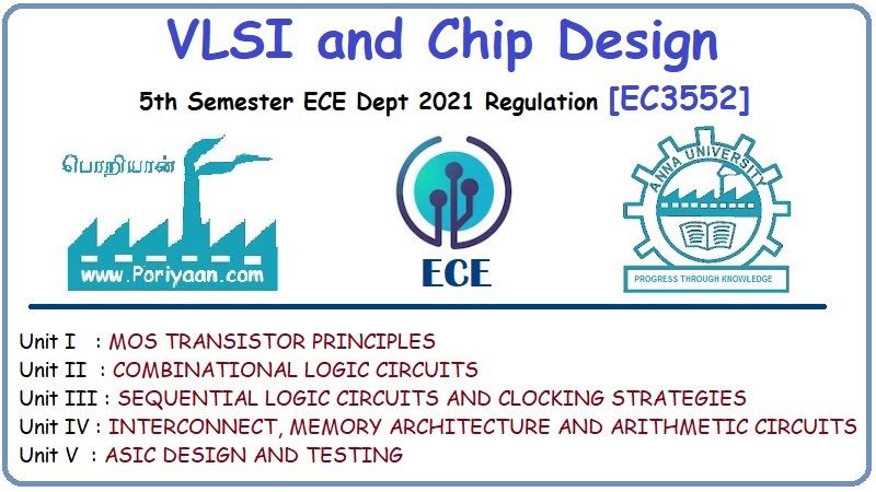
VLSI and Chip Design
EC3552 - 5th Semester - ECE Dept - 2021 Regulation
2021 regulation - 3rd year, 5th semester paper for ECE Department (Electronics and Communication Engineering Department). Subject Code: EC3552, Subject Name: VLSI and Chip Design, Batch: 2021, 2022, 2023, 2024. Institute: Anna University Affiliated Engineering College, TamilNadu. This page has VLSI and Chip Design study material, notes, semester question paper pdf download, important questions, lecture notes.
PDF Download Links
- (EC3552 2021 Regulation) VLSI and Chip Design: Semester Question Paper 2024 April May
- (EC3552 2021 Regulation) VLSI and Chip Design: Semester Question Paper 2023 Nov Dec
- (EC8095 2017 Regulation) VLSI Design: Semester Question Paper 2023 Nov Dec
- (EC8095 2017 Regulation) VLSI Design: Semester Question Paper 2022 Nov Dec
- (EC8095 2017 Regulation) VLSI Design: Semester Question Paper 2022 April May
- (EC8095 2017 Regulation) VLSI Design: Semester Question Paper 2020 Nov Dec 2021 April May
- (EC3552) VLSI and Chip Design: Hand Written Notes - Unit 5:- ASIC Design and Testing
- (EC3552) VLSI and Chip Design: Hand Written Notes - Unit 4:- Interconnect Memory Architecture and Arithmetic Circuits
- (EC3552) VLSI and Chip Design: Hand Written Notes - Unit 3:- Sequential Logic Circuits and Clocking Strategies
- (EC3552) VLSI and Chip Design: Hand Written Notes - Unit 2:- Combinational Logic Circuits
- (EC3552) VLSI and Chip Design: Hand Written Notes - Unit 1:- MOS Transistor Principles
- EC3552 VLSI and Chip Design Reg2021 Notes PDF Download
- EC3552 VLSI and Chip Design Reg2021 Notes Unit I and III PDF Download
- (EC3552) VLSI and Chip Design: Important Questions with Answer - Unit 5:- ASIC Design and Testing
- (EC3552) VLSI and Chip Design: Important Questions with Answer - Unit 4:- Interconnect Memory Architecture and Arithmetic Circuits
- (EC3552) VLSI and Chip Design: Important Questions with Answer - Unit 3:- Sequential Logic Circuits and Clocking Strategies
- (EC3552) VLSI and Chip Design: Important Questions with Answer - Unit 2:- Combinational Logic Circuits
- (EC3552) VLSI and Chip Design: Important Questions with Answer - Unit 1:- MOS Transistor Principles
VLSI and Chip Design
Notes and Question Answer of Unit I: MOS Transistor Principles will Uploaded shortly...
Notes and Question Answer of Unit II: Combinational Logic Circuits will Uploaded shortly...
Notes and Question Answer of Unit III: Sequential Logic Circuits and Clocking Strategies will Uploaded shortly...
Notes and Question Answer of Unit IV: Interconnect, Memory Architecture and Arithmetic Circuits will Uploaded shortly...
Notes and Question Answer of Unit V: ASIC Design and Testing will Uploaded shortly...
PDF Download Links
- (EC3552 2021 Regulation) VLSI and Chip Design: Semester Question Paper 2024 April May
- (EC3552 2021 Regulation) VLSI and Chip Design: Semester Question Paper 2023 Nov Dec
- (EC8095 2017 Regulation) VLSI Design: Semester Question Paper 2023 Nov Dec
- (EC8095 2017 Regulation) VLSI Design: Semester Question Paper 2022 Nov Dec
- (EC8095 2017 Regulation) VLSI Design: Semester Question Paper 2022 April May
- (EC8095 2017 Regulation) VLSI Design: Semester Question Paper 2020 Nov Dec 2021 April May
- (EC3552) VLSI and Chip Design: Hand Written Notes - Unit 5:- ASIC Design and Testing
- (EC3552) VLSI and Chip Design: Hand Written Notes - Unit 4:- Interconnect Memory Architecture and Arithmetic Circuits
- (EC3552) VLSI and Chip Design: Hand Written Notes - Unit 3:- Sequential Logic Circuits and Clocking Strategies
- (EC3552) VLSI and Chip Design: Hand Written Notes - Unit 2:- Combinational Logic Circuits
- (EC3552) VLSI and Chip Design: Hand Written Notes - Unit 1:- MOS Transistor Principles
- EC3552 VLSI and Chip Design Reg2021 Notes PDF Download
- EC3552 VLSI and Chip Design Reg2021 Notes Unit I and III PDF Download
- (EC3552) VLSI and Chip Design: Important Questions with Answer - Unit 5:- ASIC Design and Testing
- (EC3552) VLSI and Chip Design: Important Questions with Answer - Unit 4:- Interconnect Memory Architecture and Arithmetic Circuits
- (EC3552) VLSI and Chip Design: Important Questions with Answer - Unit 3:- Sequential Logic Circuits and Clocking Strategies
- (EC3552) VLSI and Chip Design: Important Questions with Answer - Unit 2:- Combinational Logic Circuits
- (EC3552) VLSI and Chip Design: Important Questions with Answer - Unit 1:- MOS Transistor Principles
VLSI and Chip Design
Unit I: MOS Transistor Principles
Notes and Question Answer of Unit I: MOS Transistor Principles will Uploaded shortly...
Unit II: Combinational Logic Circuits
Notes and Question Answer of Unit II: Combinational Logic Circuits will Uploaded shortly...
Unit III: Sequential Logic Circuits and Clocking Strategies
Notes and Question Answer of Unit III: Sequential Logic Circuits and Clocking Strategies will Uploaded shortly...
Unit IV: Interconnect, Memory Architecture and Arithmetic Circuits
Notes and Question Answer of Unit IV: Interconnect, Memory Architecture and Arithmetic Circuits will Uploaded shortly...
Unit V: ASIC Design and Testing
Notes and Question Answer of Unit V: ASIC Design and Testing will Uploaded shortly...
PDF Download Links
- (EC3552 2021 Regulation) VLSI and Chip Design: Semester Question Paper 2024 April May
- (EC3552 2021 Regulation) VLSI and Chip Design: Semester Question Paper 2023 Nov Dec
- (EC8095 2017 Regulation) VLSI Design: Semester Question Paper 2023 Nov Dec
- (EC8095 2017 Regulation) VLSI Design: Semester Question Paper 2022 Nov Dec
- (EC8095 2017 Regulation) VLSI Design: Semester Question Paper 2022 April May
- (EC8095 2017 Regulation) VLSI Design: Semester Question Paper 2020 Nov Dec 2021 April May
- (EC3552) VLSI and Chip Design: Hand Written Notes - Unit 5:- ASIC Design and Testing
- (EC3552) VLSI and Chip Design: Hand Written Notes - Unit 4:- Interconnect Memory Architecture and Arithmetic Circuits
- (EC3552) VLSI and Chip Design: Hand Written Notes - Unit 3:- Sequential Logic Circuits and Clocking Strategies
- (EC3552) VLSI and Chip Design: Hand Written Notes - Unit 2:- Combinational Logic Circuits
- (EC3552) VLSI and Chip Design: Hand Written Notes - Unit 1:- MOS Transistor Principles
- EC3552 VLSI and Chip Design Reg2021 Notes PDF Download
- EC3552 VLSI and Chip Design Reg2021 Notes Unit I and III PDF Download
- (EC3552) VLSI and Chip Design: Important Questions with Answer - Unit 5:- ASIC Design and Testing
- (EC3552) VLSI and Chip Design: Important Questions with Answer - Unit 4:- Interconnect Memory Architecture and Arithmetic Circuits
- (EC3552) VLSI and Chip Design: Important Questions with Answer - Unit 3:- Sequential Logic Circuits and Clocking Strategies
- (EC3552) VLSI and Chip Design: Important Questions with Answer - Unit 2:- Combinational Logic Circuits
- (EC3552) VLSI and Chip Design: Important Questions with Answer - Unit 1:- MOS Transistor Principles
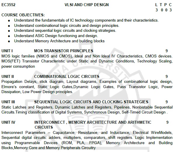
EC3552
VLSI AND CHIP DESIGN
COURSE OBJECTIVES:
i. Understand the fundamentals
of IC technology components and their characteristics.
ii. Understand combinational
logic circuits and design principles.
iii. Understand sequential
logic circuits and clocking strategies.
iv. Understand ASIC Design
functioning and design.
v. Understand Memory Architecture
and building blocks
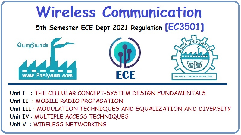
UNIT I
MOS TRANSISTOR PRINCIPLES
MOS logic families
(NMOS and CMOS), Ideal and Non Ideal IV Characteristics, CMOS devices. MOS(FET)
Transistor Characteristic under Static and Dynamic Conditions, Technology
Scaling, power consumption
UNIT II
COMBINATIONAL LOGIC CIRCUITS
Propagation Delays, stick
diagram, Layout diagrams, Examples of combinational logic design, Elmore’s constant,
Static Logic Gates,Dynamic Logic Gates, Pass Transistor Logic, Power Dissipation,
Low Power Design principles.
UNIT III
SEQUENTIAL LOGIC CIRCUITS AND CLOCKING STRATEGIES
Static Latches and
Registers, Dynamic Latches and Registers, Pipelines, Nonbistable Sequential Circuits.Timing
classification of Digital Systems, Synchronous Design, Self-Timed Circuit Design
.
UNIT IV
INTERCONNECT, MEMORY ARCHITECTURE AND ARITHMETIC
CIRCUITS
Interconnect Parameters
– Capacitance, Resistance, and Inductance, Electrical WireModels, Sequential
digital circuits: adders, multipliers, comparators, shift registers. Logic
Implementation using Programmable Devices (ROM, PLA, FPGA), Memory Architecture
and Building Blocks,Memory Core and Memory Peripherals Circuitry
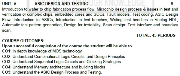
UNIT V
ASIC DESIGN AND TESTING
Introduction to wafer
to chip fabrication process flow. Microchip design process & issues in test
and verification of complex chips, embedded cores and SOCs, Fault models, Test
coding. ASIC Design Flow, Introduction to ASICs, Introduction to test benches,
Writing test benches in Verilog HDL, Automatic test pattern generation, Design
for testability, Scan design: Test interface and boundary scan.
TOTAL:
45 PERIODS
COURSE OUTCOMES:
Upon successful
completion of the course the student will be able to
CO1:
In depth knowledge of MOS technology
CO2:
Understand Combinational Logic Circuits and Design Principles
CO3:
Understand Sequential Logic Circuits and Clocking Strategies
CO4:
Understand Memory architecture and building blocks
CO5:
Understand the ASIC Design Process and Testing.
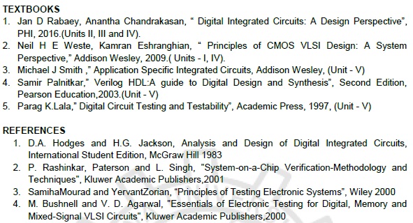
TEXTBOOKS
i. Jan D Rabaey, Anantha
Chandrakasan, “ Digital Integrated Circuits: A Design Perspective”, PHI, 2016.(Units
II, III and IV).
ii. Neil H E Weste, Kamran
Eshranghian, “ Principles of CMOS VLSI Design: A System Perspective,” Addison Wesley,
2009.( Units - I, IV).
iii. Michael J Smith ,”
Application Specific Integrated Circuits, Addison Wesley, (Unit - V)
iv. Samir Palnitkar,” Verilog
HDL:A guide to Digital Design and Synthesis”, Second Edition, Pearson Education,2003.(Unit
- V)
v. Parag K.Lala,” Digital
Circuit Testing and Testability”, Academic Press, 1997, (Unit - V)
REFERENCES
i. D.A. Hodges and H.G.
Jackson, Analysis and Design of Digital Integrated Circuits, International Student
Edition, McGraw Hill 1983
ii. P. Rashinkar, Paterson
and L. Singh, "System-on-a-Chip Verification-Methodology and Techniques",
Kluwer Academic Publishers,2001
iii. SamihaMourad and YervantZorian,
“Principles of Testing Electronic Systems”, Wiley 2000
iv. M. Bushnell and V. D.
Agarwal, "Essentials of Electronic Testing for Digital, Memory and Mixed-Signal
VLSI Circuits", Kluwer Academic Publishers,2000
VLSI and Chip Design: Unit I: MOS Transistor Principles,, VLSI and Chip Design: Unit II: Combinational Logic Circuits,, VLSI and Chip Design: Unit III: Sequential Logic Circuits and Clocking Strategies,, VLSI and Chip Design: Unit IV: Interconnect, Memory Architecture and Arithmetic Circuits,, VLSI and Chip Design: Unit V: ASIC Design and Testing,, 5th Semester ECE Dept 2021 Regulation : EC3552 - 5th Semester - ECE Dept - 2021 Regulation VLSI and Chip Design