Digital Principles and Computer Organization: Chapter 6: Sequential Circuits - Counters
Ripple / Asynchronous Counters
Questions: 1. Explain in detail the operation of a 4-bit binary ripple counter. 2. Explain the working of asynchronous down counter. 3. Design and explain the working of an up-down ripple counter. 4. What do you mean by asynchronous counter? 5. State the problem faced by ripple counters. 6. What is the primary disadvantage of asynchronous counter?
Ripple / Asynchronous
Counters
•
A binary ripple / asynchronous counter consists of a series connection of
complementing flip–flops, with the output of each flip–flop connected to the
clock input of the next higher–order flip–flop. The flip–flop holding the least
significant bit receives the incoming clock pulses. A complementing flip–flops
can be obtained from a JK flip–flop with the J and K inputs tied together as
shown in Fig. 6.2.1 or from a T flip–flop. A third alternative is to use a D
flip–flop with the complement output connected to the D input. In this way, the
D input is always the complement of the present state and the next clock pulse
will cause the flip–flop to complement. Let us see the ripple counter using JK
flip–flop.
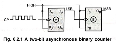
•
Fig. 6.2.1 shows 2–bit asynchronous counter using JK flip–flops. As shown in
Fig. 6.2.1, the clock signal is connected to the clock input of only first
stage flip–flop. The clock input of the second stage flip–flop is triggered by
the QA output of the first stage. Because of the inherent
propagation delay time through a flip–flop, a transition of the input clock
pulse and a transition of the QA output of first stage can never
occur at exactly the same time. Therefore, the two flip–flops are never
simultaneously triggered, which results in asynchronous counter operation.
•
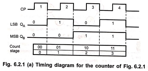
Fig. 6.2.1 (a) shows the timing diagram for two–bit asynchronous counter. It
illustrates the changes in the state of the flip–flop outputs in response to
the clock. J and K input of JK flip–flops are tied to logic HIGH hence output
will toggle for each negative edge of the clock input.
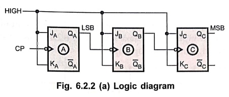
Example: 1
Extend the counter
shown in Fig. 6.2.2 for 3–stages, and draw output waveforms.
Solution :
In
Fig. 6.2.2 (b), timing diagram for 3–bit asynchronous counter we have not
considered the propagation delays of flip–flops, for simplicity. If we consider
the propagation delays of flip–flops we get timing diagram as shown in Fig.
6.2.3.
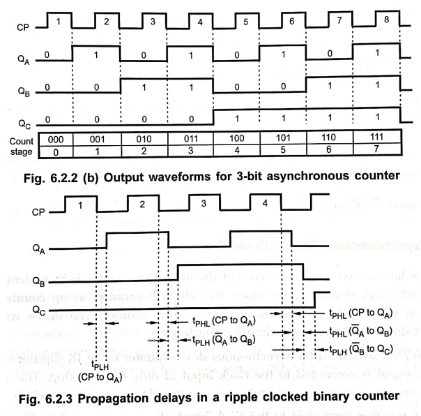
The
timing diagram shows propagation delays. We can see that propagation delay of the
first stage is added in the propagation delay of second stage to decide the
transition time for third stage. This cumulative delay of an asynchronous
counter is a major disadvantage in many applications because it limits the rate
at which the counter can be clocked and creates decoding problems.
Example: 2
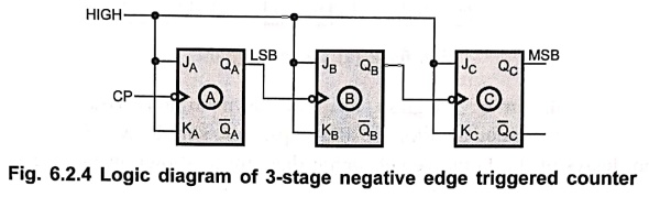
Draw the logic diagram
for 3–stage asynchronous counter with negative edge triggered flip–flops.
Solution :
When
flip–flops are negatively edge triggered, the Q output of previous stage is
connected to the clock input of the next stage. Fig. 6.2.4 shows 3–stage
asynchronous counter with negative edge triggered flip–flops.
Example: 3
A counter has 14 stable
states 0000 through 1101. If the input frequency is 50 kHz what will be its
output frequency?
Solution :
50
kHz / 14 = 3.57 kHz
Example: 4
The tpd for
each flip–flop is 50 ns, determine the maximum operating frequency for MOD–32
ripple counter.
Solution :
We
know that MOD–32 uses five flip–flops. With tpd = 50 ns, the fmax
for ripple counter can be given as,
fmax
(ripple) = 1 / (5 × 50 ns ) =
4 MHz
1. Asynchronous / Ripple Down Counter
•
In the last section we have seen that the output of counter is incremented by
one for each clock transition. Therefore, we call such counters as up counters. In this section we see the
asynchronous / ripple down counter. The down counter will count downward from a
maximum count to zero.
•
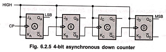
Fig. 6.2.5 shows the 4–bit asynchronous down counter using JK flip–flops. Here,
the clock signal is connected to the clock input of only first flip–flop. This
connection is same as asynchronous / ripple up counter. However, the clock
input of the remaining flip–flops is triggered by the  A
output of the previous stage instead of QA output of the previous
stage.
A
output of the previous stage instead of QA output of the previous
stage.
•
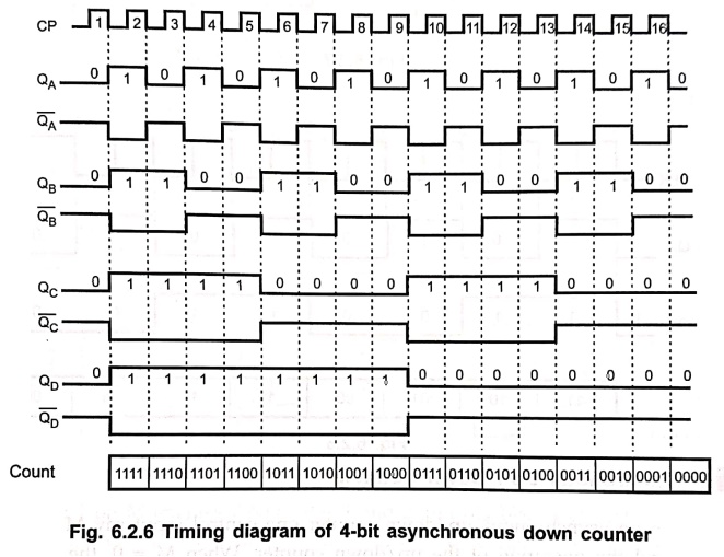
Fig. 6.2.6 shows the timing diagram for 4–bit asynchronous down counter. It
illustrates the changes in the state of the flip–flop outputs in response to
the clock. Again the J and K inputs of JK flip–flops are tied to logic HIGH
hence output will toggle for each negative edge of the clock input.
•
Down counters are not as widely used as up counters. They are used in
situations. where it must be known when a desired number of input pulses has
occurred. In these situations the down counter is preset to the desired number
and then allowed to count down as the pulses are applied. When the counter
reaches the zero state it is detected by a logic gate whose output then
indicates that the preset number of pulses have occurred.
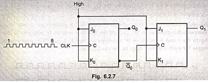
Example: 5
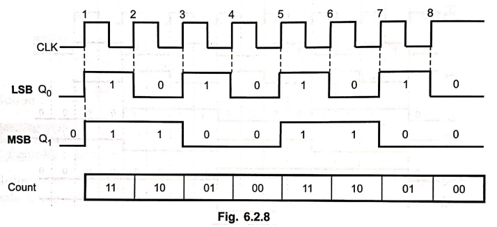
For the ripple counter
shown in Fig. 6.2.7, show the complete timing diagram for eight clock pulses,
showing the clock, Q0 and Q1 waveforms.
Solution :
2. Asynchronous Up/Down Counter
•
To form an asynchronous up / down us up/down counter one control input say M is
necessary to control the operation of the up / down counter. When M = 0, the
counter will count down and when M = 1, the counter will count up.
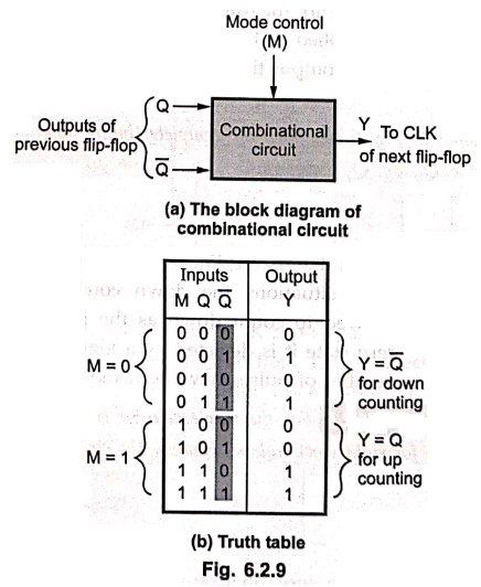
(a) The block diagram of combinational circuit, (b) Truth table
To
achieve this the M input should be used to control whether the normal flip–flop
output (Q) or the inverted flip–flop output () is fed to drive
the clock signal of the successive stage flip–flop, as shown in Fig. 6.2.9 (a).
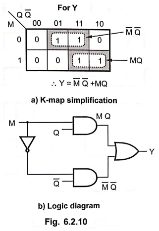
The truth table for such combinational circuit is shown in Fig. 6.2.9 (b).
a) K–map simplification, b) Logic diagram
•
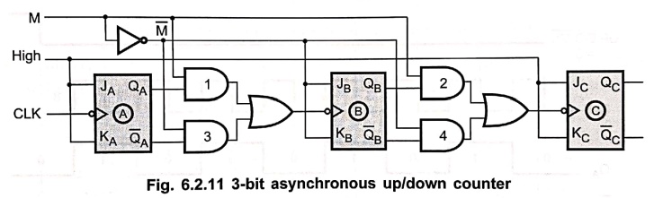
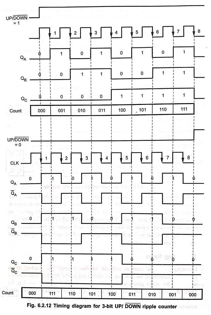
Fig. 6.2.11 shows the 3–bit up / down counter that will count from 000 up to
111 when the mode control input M is 1 and from 111 down to 000 when mode
control input M is 0.
•
A logic 1 on M enables AND gates 1 and 2 and disables AND gates 3 and 4. This
allows the QA and QB outputs to drive the clock inputs of
their respective next stages. So that counter will count up. When M is logic 0,
AND gates 1 and 2 are disabled and AND gate 3 and 4 are enabled. This allows
the A and QB
outputs to drive the clock inputs of their respective next stages so that
counter will count down. Fig. 6.2.12 shows the timing diagram for 3–bit up/down
ripple counter.
3. Decoding Gates
•
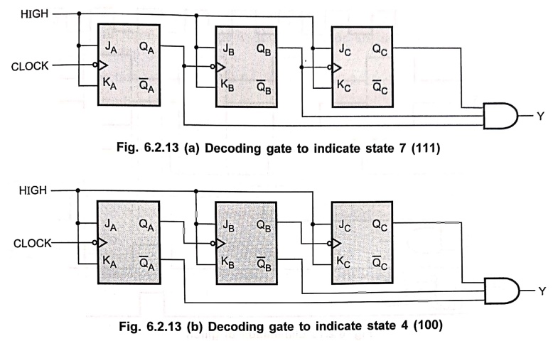
Decoding gates are used to indicate whether counter has reached to particular
state. The outputs of the counter are connected to the AND gate as inputs and
the output of the AND gate goes high for particular state. Let us see Fig.
6.2.13 (a). Here, the output of decoding gate goes high when counter outputs
are C = 1, B = 1 and A = 1. In Fig. 6.2.13 (b) the output of decoding gate goes
high when counter outputs are C = 1, B = 0 and A = 0.
•
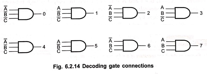
Similarly, we can connect corresponding outputs to decoding gate inputs to
indicate desired state. Fig. 6.2.14 gives these connections for all possible
state detection for 3–bit counter.
4. Problem Faced by Ripple Counters (Glitch Problem)
•
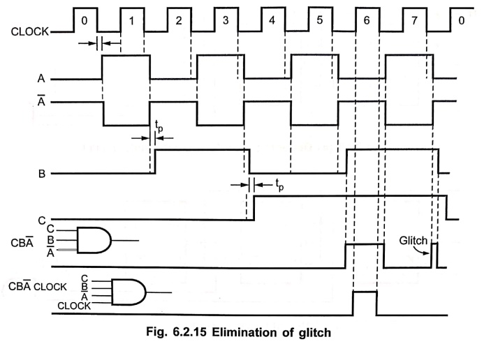
We know that, due to the propagation delay the output flip–flop is delayed by
time tp. This illustrated in the waveform shown in Fig. 6.2.15 shows
the waveform of the circuit which decodes state 6. Here, the output of flip–flop
A triggers the flip–flop B, hence the B waveform is delayed by one flip–flop
delay time (tp) the negative transition of A. Similarly, the C
waveform is delayed by tp from each negative transition of B.
•
Let us observe the output waveform when the counter progresses from state 7 to
state 0. At point X, A goes low (Ā goes high); however, because of flip–flop
delay time, B does not go low until point Y. Thus between points X and Y we
have the condition C = 1, B = 1 and A = 1. As a result, the output is high
between points X and Y. This undesirable output is known as glitch. We can avoid the glitch on the
output waveform by connecting clock as a fourth input to the decoding gate
along with inputs A, B and C. This is illustrated in Fig. 6.2.15.
Review Questions
1. Explain in detail
the operation of a 4–bit binary ripple counter.
2. Explain the working
of asynchronous down counter.
3. Design and explain
the working of an up–down ripple counter.
4. What do you mean by
asynchronous counter?
5. State the problem
faced by ripple counters.
6. What is the primary
disadvantage of asynchronous counter?
Digital Principles and Computer Organization: Chapter 6: Sequential Circuits - Counters : Tag: : - Ripple / Asynchronous Counters
Digital Principles and Computer Organization: Chapter 6: Sequential Circuits - Counters
Under Subject

Digital Principles and Computer Organization
CS25C06 2nd Semester AIDS, CSE, IT, CSE(CY) Dept | 2025 Regulation | 2nd Semester 2025 Regulation
Related Subjects

English Essentials II
EN25C02 2nd Semester | 2025 Regulation | 2nd Semester 2025 Regulation

Tamils and Technology தமிழர்களும் தொழில்நுட்பமும்
UC25H02 2nd Semester | 2025 Regulation | 2nd Semester 2025 Regulation

Linear Algebra
MA25C02 2nd Semester | 2025 Regulation

Applied Physics (CSIE) II
PH25C03 2nd Semester AIDS, CSE, IT, CSE(CY) Dept | 2025 Regulation | 2nd Semester 2025 Regulation
Digital Principles and Computer Organization
CS25C06 2nd Semester AIDS, CSE, IT, CSE(CY) Dept | 2025 Regulation | 2nd Semester 2025 Regulation

Basic Electrical and Electronics Engineering
EE25C01 2nd Semester | 2025 Regulation | 2nd Semester 2025 Regulation

Python for Data Science
AD25201 2nd Semester AIDS Dept | 2025 Regulation | 2nd Semester 2025 Regulation

Re-Engineering for Innovation
ME25C05 2nd Semester | 2025 Regulation | 2nd Semester 2025 Regulation

Python for Data Science - Laboratory
AD25201 2nd Semester AIDS Dept | 2025 Regulation | 2nd Semester 2025 Regulation