Digital Principles and Computer Organization: Chapter 6: Sequential Circuits - Counters
Synchronous Counters
Sequential Circuits
1. 2-bit Synchronous Binary Up Counter, 2. 3-bit Synchronous Binary Up Counter , 3. 4-bit Synchronous Binary Up Counter, 4. Synchronous Down and Up/Down Counters. Questions: 1. Define synchronous counter. 2. Explain the working of 3-bit synchronous binary up counter. 3. Explain the working of synchronous up/down counter. 4. Design a 3-bit synchronous counter using JK flip-flops.
Synchronous Counters
•
When counter is clocked such that each flip–flop in the counter is triggered at
the same time, the counter is called as synchronous counter.
1. 2–bit Synchronous Binary Up Counter
•
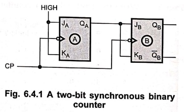
Fig. 6.4.1 show two stage synchronous counter.
•
Here, clock signal is connected in parallel to clock inputs of both the flip–flops.
But the QA output of first stage is used to drive the J and K inputs
of the second stage. Let us see the operation of the circuit. Initially, assume
that the QA = QB = 0. When positive edge of the first
clock pulse is applied, flip–flop A will toggle because JA = KA
= 1, whereas flip–flop B output will remain zero because JB = KB
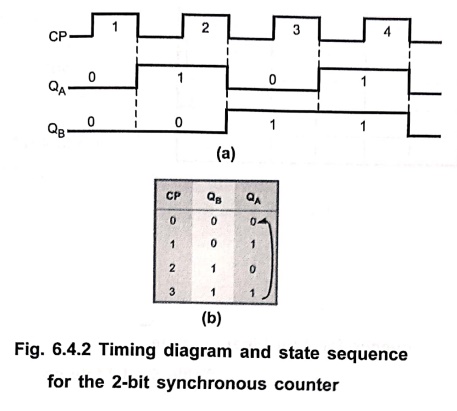
= 0. After first clock pulse QA = 1 and QB = 0. At
negative going edge of the second clock pulse both flip–flops will toggle
because they both have a toggle condition on their J and K inputs (JA
= KA= JB = KB =1). Thus after second clock
pulse, QA= 0 and QB = 1. At negative going edge of the
third clock pulse flip–flop A toggles making QA = 1, but flip–flop B
remains set i.e. QB = 1. Finally, at the leading edge of the fourth clock
pulse both flip–flops toggle as their JK inputs are at logic 1. This results QA
= QB = 0 and counter recycled back to its original state. The timing
details of above operation is shown in Fig. 6.4.2.
2. 3–bit Synchronous Binary Up Counter
Fig.
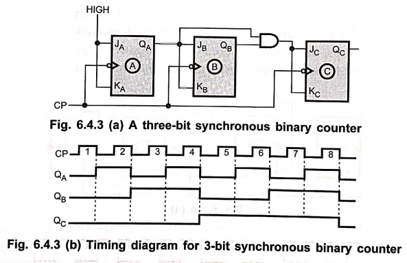
6.4.3 (a) shows 3–bit synchronous binary counter and its timing diagram. The
state sequence for this counter is shown in Table 6.4.1.
•
Looking at Fig. 6.4.3 (b), we can see that QA changes on each clock
pulse as we progress from its original state to its final state and then back
to its original state. To produce this operation, flip–flop A is held in the
toggle mode by connecting J and K inputs to HIGH. Now let us see what flip–flop
B does. Flip–flop B toggles, when QA is 1. When QA is a
0, flip–flop B is in the no–change mode and remains in its present state.
Looking at Table 6.4.1 we can notice that flip–flop C has to change its state
only when QB and QA both are at logic 1. This condition
is detected by AND gate and applied to the J and K inputs of flip–flop C.
Whenever both QA and QB are HIGH, the output of the AND
gate makes the J and K inputs of flip–flop C HIGH and flip–flop C toggles on
the following clock pulse.
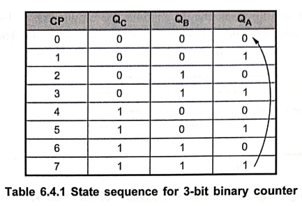
At
all other times, the J and K inputs of flip–flop C are held LOW by the AND gate
output and flip–flop does not change state.
3. 4–bit Synchronous Binary Up Counter
•
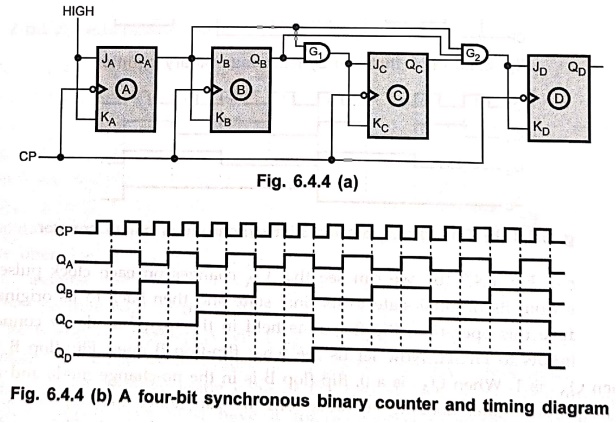
Fig. 6.4.4 (a) and (b) shows logic diagram and timing diagram for 4–bit
synchronous binary counter. As counter is implemented with negative edge
triggered flip–flops, the transitions occur at the negative edge of the clock
pulse. In this circuit, first three flip–flops work same as 3–bit counter
discussed previously.
•
For the fourth stage, flip–flop has to change the state when QA = QB
= Qc = 1. This condition is decoded by 3–input AND gate G2.
Therefore, when QA = QB = Qc = 1, flip–flop D toggles and
for all other times it is in no change condition.
Example: 1
Determine fmax for the 4–bit synchronous
counter if tpd for each flip–flop is 50 ns and tpd for
each AND gate is 20 ns. Compare this with fmax
for a MOD–16 ripple counter.
Solution :
For
a synchronous counter the total delay that must be allowed between input clock
pulses is equal to flip–flop tpd + AND gate tpd. Thus Tclock
≥ 50 + 20 = 70 ns and so the counter has
fmax
= 1 / 70 ns = 14.3 MHz
We
know that MOD–16 ripple counter used four flip–flops. With flip–flop tpd
= 50 ns, the fmax for ripple counter can be given as,
fmax (ripple) = 1 / (4 ×
50 ns) = 5 MHz
4. Synchronous Down and Up/Down Counters
•
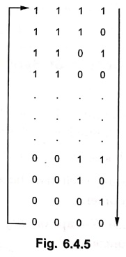
We have seen that a ripple counter could be made to count down by using the
inverted output of each flip–flop to drive the next flip–flops in the counter.
A parallel / synchronous down counter can be constructed in a similar manner
that is, by using the inverted FF outputs to drive the following JK inputs. For
example, the parallel up counter of Fig. 6.4.4 (a) can be converted to a down
counter by connecting the  ,,
,, ,
, and
and  outputs in place of QA, QB, Qc
and QD respectively. The counter will then proceed through the
following sequence as input Dijon pulses are applied :
outputs in place of QA, QB, Qc
and QD respectively. The counter will then proceed through the
following sequence as input Dijon pulses are applied :
•
To form a parallel up / down counter the control input 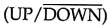 is used to control whether the
normal flip–flop outputs or the inverted flip–flop outputs are fed to the J and
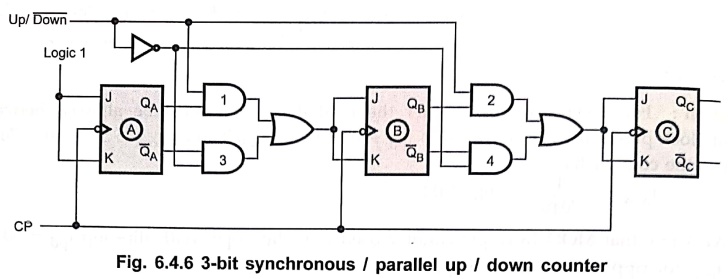
K inputs of the following flip–flops. Fig. 6.4.5 shows 3–bit up/down counter
that will count from 000 up to 111 when the control
input is 1 and from 111 down to 000 when the control input
is 0.
is used to control whether the
normal flip–flop outputs or the inverted flip–flop outputs are fed to the J and
K inputs of the following flip–flops. Fig. 6.4.5 shows 3–bit up/down counter
that will count from 000 up to 111 when the control
input is 1 and from 111 down to 000 when the control input
is 0.
•
A logic 1 on the enables AND gates 1 and 2 and
disables AND gates 3 and 4. This allows the QA and QB
outputs through to the J and K inputs of the next flip–flops so that the
counter will count up as pulses are applied. When line is logic 0, AND gates 1 and 2
are disables and AND gates 3 and 4 are enabled. This allows the and outputs through to the J and K inputs of the next
flip–flops so that the counter will count down as pulses are applied.
Review Questions
1. Define synchronous
counter.
2. Explain the working
of 3–bit synchronous binary up counter.
3. Explain the working
of synchronous up/down counter.
4. Design a 3–bit
synchronous counter using JK flip–flops.
Digital Principles and Computer Organization: Chapter 6: Sequential Circuits - Counters : Tag: : Sequential Circuits - Synchronous Counters
Digital Principles and Computer Organization: Chapter 6: Sequential Circuits - Counters
Under Subject

Digital Principles and Computer Organization
CS25C06 2nd Semester AIDS, CSE, IT, CSE(CY) Dept | 2025 Regulation | 2nd Semester 2025 Regulation
Related Subjects

English Essentials II
EN25C02 2nd Semester | 2025 Regulation | 2nd Semester 2025 Regulation

Tamils and Technology தமிழர்களும் தொழில்நுட்பமும்
UC25H02 2nd Semester | 2025 Regulation | 2nd Semester 2025 Regulation

Linear Algebra
MA25C02 2nd Semester | 2025 Regulation

Applied Physics (CSIE) II
PH25C03 2nd Semester AIDS, CSE, IT, CSE(CY) Dept | 2025 Regulation | 2nd Semester 2025 Regulation
Digital Principles and Computer Organization
CS25C06 2nd Semester AIDS, CSE, IT, CSE(CY) Dept | 2025 Regulation | 2nd Semester 2025 Regulation

Basic Electrical and Electronics Engineering
EE25C01 2nd Semester | 2025 Regulation | 2nd Semester 2025 Regulation

Python for Data Science
AD25201 2nd Semester AIDS Dept | 2025 Regulation | 2nd Semester 2025 Regulation

Re-Engineering for Innovation
ME25C05 2nd Semester | 2025 Regulation | 2nd Semester 2025 Regulation

Python for Data Science - Laboratory
AD25201 2nd Semester AIDS Dept | 2025 Regulation | 2nd Semester 2025 Regulation