Basic Electronics and Electrical Engineering: Practical Experimentation
To plot Volt‒Ampere Characteristics of P-N Junction Diode
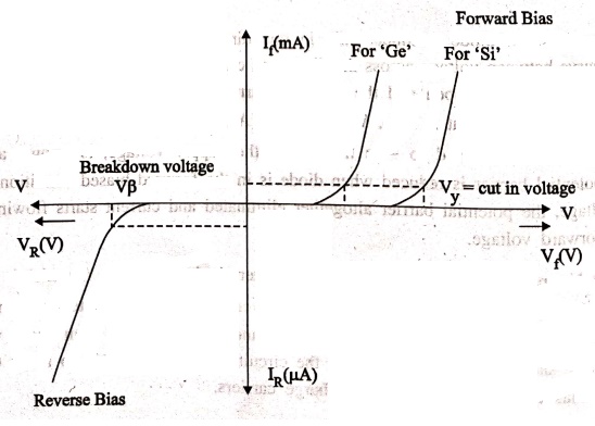
PN Junction diode characteristics (A) Forward bias (B) Reverse bias
PN Junction diode characteristics
(A) Forward bias (B) Reverse bias
Aim
1. To plot Volt‒Ampere
Characteristics of P‒N Junction Diode.
Apparatus
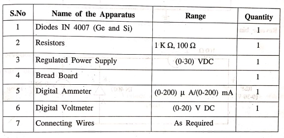
Theory
A p‒n junction diode
conducts only in one direction. The V‒I characteristics of the diode are curve
between voltage across the diode and current through the diode. When external
voltage is zero, circuit is open and the potential barrier does not allow the
current to flow. Therefore, the circuit current is zero. When P‒type (Anode is
connected to + ve terminal and n‒type (cathode) is connected to ‒ve thermal of
the supply voltage, is known as forward bias. The potential barrier is reduced
when diode is in the reduced when diode is in the forward biased condition. At
some forward voltage, the potential barrier altogether eliminated and current
starts flowing through the diode forward voltage.
When N‒type (cathode)
is connected to + ve terminal and P‒type (Anode) is connected ‒ ve terminal of
the supply voltage is known as reverse bias and the potential barrier across
the junction increases. Therefore, the junction resistance becomes very high
and a very small current (reverse saturation current) flows in the circuit. The
diode is said to be in OFF state. The reverse bias current due to minority
charge carriers.
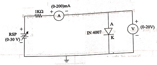
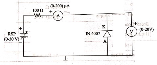
Circuit diagram
(i)
Forward bias
(ii)
Reverse bias
V‒I Characteristics
Procedure
(i)
Forward bias (For 'Ge' and 'Si' Diode)
1. Connections are made
as per the circuit diagram.
2. For forward bias,
the RPS +ve is connected to the anode of the diode and RPS ‒ ve is connected to
the cathode of the diode,
3. Switch ON the power
supply and increases the input voltage (supply voltage) in Steps.
4. Note down the
corresponding current flowing through the diode and voltage across the diode
for each and every step of the input voltage.
5. The readings of
voltage and current are tabulated.
6. Graph is plotted
between voltage on x‒axis and current
on y‒axis.
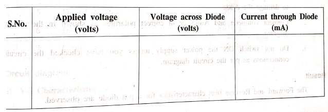
Observations
Forward
bias
Procedure
i)
Reverse bias
1. Connections are made
as per the circuit diagram.
2. For reverse bias,
the RPS +ve is connected to the cathode of the diode and RPS ‒ve is connected to
the anode of the diode.
3. Switch ON the power
supply and increase the input voltage (supply voltage) in Steps.
4. Note down the
corresponding current flowing through the diode and voltage across the diode
for each and every step of the input voltage.
5. The readings of
voltage and current are tabulated.
6. The Graph is plotted
between voltage on x‒axis and current
on y‒axis.
Observations
Reverse
bias

Precautions
1. While doing the
experiment do not exceed the rating of the diode. This may lead to damage the
diode.
2. Connect voltmeter
and Ammeter in correct polarities as shown in the circuit diagram.
3. Do not switch ON the
power supply unless you have checked the circuit connections as per the circuit
diagram.
Result
The Forward and Reverse
bias characteristics for a p‒n diode are observed.
Basic Electronics and Electrical Engineering: Practical Experimentation : Tag: Basic Engineering : - To plot Volt‒Ampere Characteristics of P-N Junction Diode
Basic Electronics and Electrical Engineering: Practical Experimentation
Under Subject

Basic Electronics and Electrical Engineering
EE25C04 1st Semester ECE Dept | 2025 Regulation | 2nd Semester 2025 Regulation
Related Subjects

English Essentials I
EN25C01 1st Semester | 2025 Regulation | 1st Semester 2025 Regulation

தமிழர் மரபு - Heritage of Tamils
UC25H01 1st Semester | 2025 Regulation | 1st Semester 2025 Regulation
Applied Calculus
MA25C01 Maths 1 M1 - 1st Semester | 2025 Regulation | 1st Semester 2025 Regulation

Applied Physics I
PH25C01 1st Semester | 2025 Regulation | 1st Semester 2025 Regulation

Applied Chemistry I
CY25C01 1st Semester | 2025 Regulation | 1st Semester 2025 Regulation

Makerspace
ME25C04 1st Semester | 2025 Regulation | 1st Semester 2025 Regulation

Computer Programming C
CS25C01 1st Semester | 2025 Regulation | 1st Semester 2025 Regulation

Computer Programming Python
CS25C02 1st Semester | 2025 Regulation | 1st Semester 2025 Regulation
Fundamentals of Electrical and Electronics Engineering
EE25C03 1st Semester | 2025 Regulation | 1st Semester 2025 Regulation
Introduction to Mechanical Engineering
ME25C03 1st Semester | 2025 Regulation | 1st Semester 2025 Regulation

Introduction to Civil Engineering
CE25C01 1st Semester Civil Department | 2025 Regulation | 1st Semester 2025 Regulation
Essentials of Computing
CS25C03 1st Semester - AID CSE IT Department | 2025 Regulation | 1st Semester 2025 Regulation

Applied Physics I Laboratory
PH25C01 1st Semester practical Laboratory Manual | 2025 Regulation | 1st Semester Laboratory 2025 Regulation

Applied Chemistry I Laboratory
CY25C01 1st Semester practical Laboratory Manual | 2025 Regulation | 1st Semester Laboratory 2025 Regulation

Computer Programming C Laboratory
CS25C01 1st Semester practical Laboratory Manual | 2025 Regulation | 1st Semester Laboratory 2025 Regulation

Computer Programming Python Laboratory
CS25C02 1st Semester practical Laboratory Manual | 2025 Regulation | 1st Semester Laboratory 2025 Regulation
Engineering Drawing
ME25C01 EEE Mech Dept | 2025 Regulation | 2nd Semester 2025 Regulation
Basic Electronics and Electrical Engineering
EE25C04 1st Semester ECE Dept | 2025 Regulation | 2nd Semester 2025 Regulation