Digital Principles and Computer Organization: Chapter 5: Sequential Circuits - Flip-Flops
Flip-Flops
1. Latches Vs Flip-Flops, 2 Level and Edge Triggering, 3. SR Flip-Flop, 4. D Flip-Flop, 5. JK Flip-Flop, 6. Master-Slave SR Flip-Flop, 7. Master-Slave JK Flip-Flop, 8. T Flip-Flop, 9 Asynchronous or Direct Inputs. Questions: 1. Explain the working of a master-slave JK flip-flop. 2. Realize a SR flip-flop using NAND gates and explain its operation. 3. Derive the characteristic equation of a SR flip-flop. 4. With reference to a JK flip-flop, what is racing? 5. Differentiate between flip-flop and latch. 6. Describe the input and output action of JK master/slave flip-flops. 7. Draw the circuit for SR flip-flop. 8. Realize SR flip-flop using NOR gates and explain its operation. 9. Draw RS flipflop circuit and explain its operation with truth table and suggest how to eliminate the undetermined stage? Write some RS flipflop applications. 10. Explain the operation of JK master slave flip-flop with suitable diagrams. 11. What is the drawback of SR flip-flop? How is this minimized? 12. Explain the working of JK flip-flop. 13. What is race around condition and how is it overcome? Explain these concepts with relevant timing diagrams. 14. Draw the clocked RS flip-flop and explain with truth table. 15. How does a JK flip-flop differ from the SR flip-flop in its basic operation? 16. Draw the logic symbol and truth table of a D flip-flop. 17. Derive the characteristic equation of a D flip flop. 18. Draw the logic circuit of a clocked JK flip-flop. 19. Draw the logic diagram of a D-FF using NAND gates and explain. 20. Mention any two differences between the edge triggering and level triggering. 21. Write down the characteristic equation and truth table for the JK flip-flop. 22. Mention the major application of master slave flip-flop. 23. Explain the different types of triggering with waveforms. 24. Draw and explain the working of clocked D flip-flop. 25. How can race condition be avoided in flip-flop ? 26. Explain the T flip-flop. 27. Explain the operation of master-slave SR flip-flop. 28. Explain the use of asynchronous inputs. 29. Draw the block diagram of SR-FF and explain. 30. Explain the operation of JK flip-flop with neat diagram.
Flip–Flops
1. Latches Vs Flip–Flops
•
Latches and flip–flops are the basic building blocks of the most sequential
circuits. The main difference between latches and flip–flops is in the method
used for changing their state.
•
A simple latch forms the basis for the flip–flop. Latches are controlled by
enable signal, and they are level triggered, either positive level triggered or
negative level triggered. The output state is free to change according to the S
and R input values, when active level is maintained at the enable input. Flip–flops
are different from latches. Flip–flops are pulse or clock edge triggered instead
of level triggered.
2. Level and Edge Triggering
Level
triggering
•
In the level triggering, the output state is allowed to change according to
input(s) when active level (either positive or negative) is maintained at the
enable input. There are two types of level triggered latches :
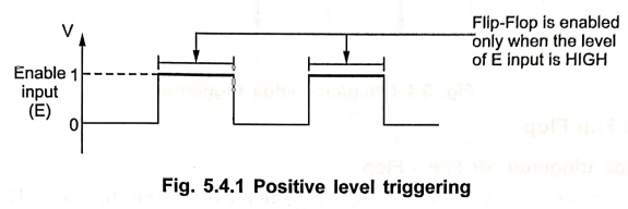
• Positive level
triggered : The output of flip–flop responds to the
input changes only when its enable input is 1 (HIGH).
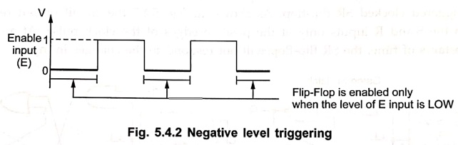
• Negative level
triggered : The output of flip–flop responds to the
input changes only when its enable input is 0 (LOW).
Edge
triggering
In
the edge triggering, the output responds to the changes in the input only at
the positive or negative edge of the clock pulse at the clock input. There are
two types of edge triggering.
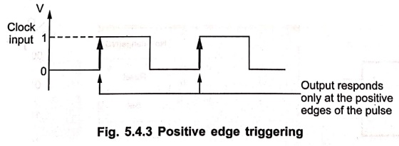
• Positive edge
triggering : Here, the output responds to the
changes in the input only at the positive edge of the clock pulse at the clock
input.
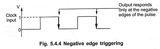
• Negative edge
triggering : Here, the output responds to the
changes in the input only at the negative edge of the clock pulse at the clock
input.
3. SR Flip–Flop
Positive edge triggered SR Flip–Flop
•
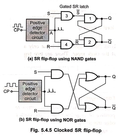
Fig. 5.4.5 shows the positive edge triggered clocked SR flip–flop. The circuit
is similar to SR latch except enable signal is replaced by the Clock Pulse (CP)
followed by the positive edge detector circuit. The edge detector circuit is a
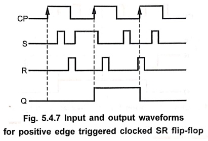
differentiator. Fig. 5.4.7 shows input and output waveforms for positive edge
triggered clocked SR flip–flop. As shown in Fig. 5.4.7 the circuit output
responds to the Sand R inputs only at the positive edges of the clock pulse. At
any other instants of time, the SR flip–flop will not respond to the changes in
input.
(a) SR flip–flop using NAND gates
(b) SR flip–flop using
NOR gates
•
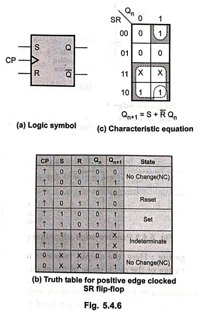
Fig. 5.4.6 shows the logic symbol and truth table of clocked SR flip–flop.
(a) Logic symbol
(b) Truth table for
positive edge clocked SR flip–flop
(c) Characteristic
equation
Case 1: If
S = R = 0 and the clock pulse is
applied, the output do not change, i.e. Qn + 1 = Qn. This
is indicated in the first row of the truth table.
Case 2 :
If S = 0, R = 1 and the clock pulse is
applied, Qn + 1 = 0. This is indicated in the second row of the truth
table.
Case 3 :
If S = 1, R = 0 and the clock pulse is applied, Qn + 1 = 1. This is
indicated in the third row of the truth table.
Case 4 : If
S = R = 1 and the clock pulse is applied, the state of the flip–flip is
undefined and therefore is indicated as indeterminate in the fourth row of the
truth table.
Negative edge triggered SR flip–flop
•
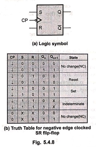
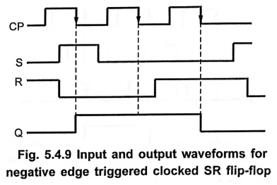
In the negative edge triggered SR flip–flop, the negative edge detector circuit
is Aused and the circuit output responds at the negative edges of the clock
pulse. Fig. 5.4.8 and Fig. 5.4.9 shows the logic symbol, truth table, and input
and output 0x waveforms for negative edge triggered SR flip–flop. The bubble at
the clock input indicates that the flip–flop is negative edge triggered.
(a) Logic symbol
(b) Truth Table for
negative edge clocked SR flip–flop
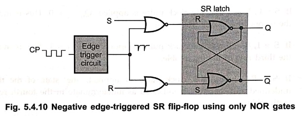
Example: 1
Realize SR flip–flop
using NOR gates.
Solution :
4. D Flip–Flop
•
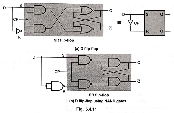
Fig. 5.4.11 shows the logic diagrams of D flip–flop. The basic building block
of D flip–flop is a SR flip–flop. The SR flip–flop has two data inputs S and R.
The S input is made high to store 1 in the flip–flop and R input is made high
to store 0 in the flip–flop.
•
Looking at the truth table of the SR flip–flop we can realize that when both
inputs are same the output either does not change or it is invalid (Inputs →
00, no change and inputs→ 11, invalid). In many practical applications, these
input conditions are not required. These input conditions can be avoided by
making them complement of each other. This modified SR flip–flop is known as D
flip–flop.
•
As shown in Fig. 5.4.11, the D input goes directly to the S input, and its
complement is applied to the R input. Due to these connections, only two input
conditions exists, either S = 0 and R = 1 or S = 1 and R = 0. The truth table
for D flip–flop consider only these two conditions and it is as shown in Fig.
5.4.12 (b).
(a) SR flip–flop - D
flip–flop
(b) SR flip–flop - D
flip–flop using NAND gates
•
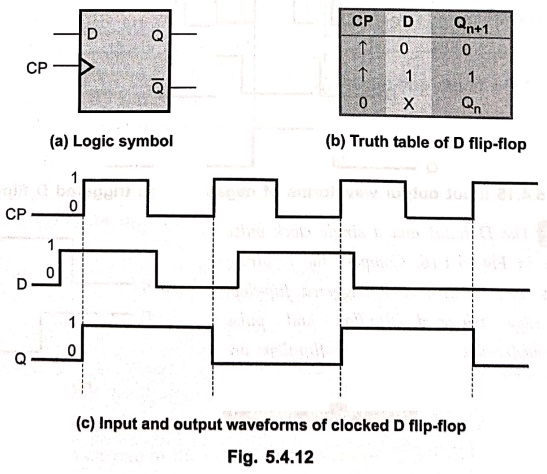
Looking at the truth table for D flip–flop we can realize that Qn+1
function follows D input at the positive going edges of the clock pulses. Hence
the characteristic equation for D flip–flop is Qn+1 = D. However,
the output Qn+1 is delayed by one clock period. Thus, D flip–flop is
also known as delay flip–flop.
(a) Logic symbol
(b) Truth table of D
flip–flop
(c) Input and output
waveforms of clocked D flip–flop
•
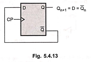
If we connect the  output of D flip–flop to its D input as shown in
Fig. 5.4.13, the output of D flip–flop will change either from 0 to 1 or from 1
to 0 at every positive edge of the D flip–flop.
output of D flip–flop to its D input as shown in
Fig. 5.4.13, the output of D flip–flop will change either from 0 to 1 or from 1
to 0 at every positive edge of the D flip–flop.
•
Such change in the output is known as toggling
of the flip–flop output.
Negative edge triggered D flip–flop
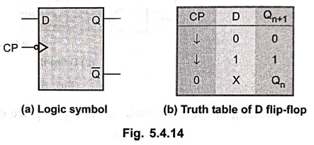
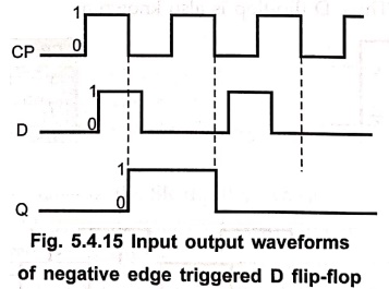
• In the previous explanation we have seen the output of D flip–flop is sensitive at the positive edge of the clock input. In case of negative edge triggering, the output is sensitive at the negative edge of the clock input. Fig. 5.4.14 shows the logic symbol and truth table for negative edge triggered D flip–flop and Fig. 5.4.15 shows input and output waveforms for negative edge triggered D flip–flop. The bubble at the clock input indicates that the flip–flop is bnegative edge triggered.
(a) Logic symbol
(b) Truth table of D
flip–flop
Example: 2
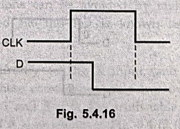
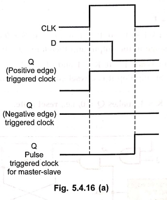
The D input and a
single clock pulse are shown in Fig. 5.4.16. Compare the resulting Q outputs
for : Positive edge triggered flip–flop, negative edge triggered flip–flop and
pulse triggered master–slave flip–flops. The flip–flops are initially RESET.
Solution :
5. JK Flip–Flop
•
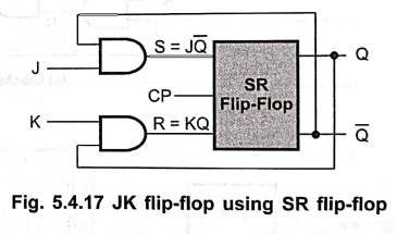
The uncertainty in the state of an SR flip–flop when S= R = 1 can be eliminated
by converting it into a JK flip–flop. The data inputs are J and K which are
ANDed with Q and Q, respectively, to obtain S and R inputs, as shown in Fig.
5.4.17. Thus, S = J. and R = K .Q.
Let
us see the operation of JK flip–flop.
Case : 1 J = K = 0
When
J = K = 0, S = R = 0 and according to truth table of SR flip–flop there is no
change in the output.
When
inputs J = K = 0, output does not change.
Case 2 : J = 1 and K =
0
Q
= 0, = 1: When J = 1, K = 0 and Q =0 , S = 1 and R = 0. According
to truth table of SR flip–flop it is set state and the output Q will be 1.
Q
= 1, = 0 : When J = 1, K = 0 and Q = 1, S = 0 and R = 0. Since SR
= 00, there is no change in the output and therefore, Q = 1 and = 0.
The inputs J = 1 and K
= 0, makes Q = 1, i.e. set state.
Case 3 : J = 0 and K =
1
Q
= 0, = 1 : When J = 0, K = 1 and Q = 0, S = 0 and R = 0. Since
SR = 00, there is no change in the
output and therefore, Q = 0 and = 1.
Q
= 1, = 0 : When J = 0, K = 1 and Q = 1, S = 0 and R = 1. According
to truth table of SR flip–flop it is a reset
state and the output Q will be 0.
The inputs J = 0 and K
= 1, makes Q = 0, i.e., reset state.
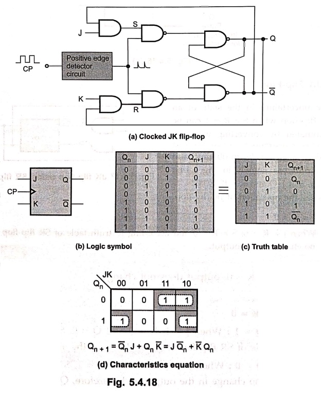
(a) Clocked JK flip–flop, (b) Logic symbol, (c) Truth table, (d) Characteristics equation
Case 4 : J = K = 1
Q
= 0, = 1 : When J = K = 1 and Q = 0, S = 1 and R = 0. According
to truth table of SR flip–flop it is a set state and the output Q will be 1.
Q
= 1, = 0: When J = K = 1 and Q = 1, S= 0 and R = 1. According to truth table of SR flip–flop it is
a reset state and the output Q will be 0.
The input J = K = 1,
toggles the flip–flop output.
•
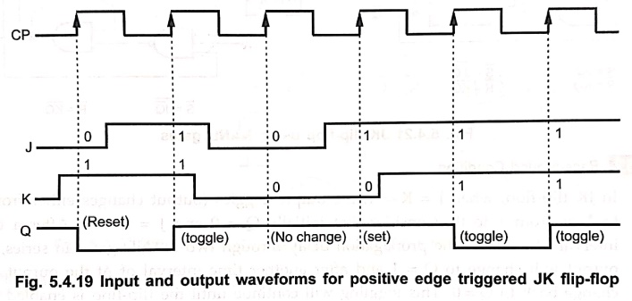
Fig. 5.4.18 shows the logic symbol, truth table and Fig. 5.4.19 shows timing diagram
of positive edge triggered JK flip–flop.
Example: 3
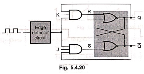
Construct a clocked JK
flip–flop which is triggered at the positive edge of the clock pulse from a
clocked SR flip–flop consisting of NOR gates.
Solution :
1. JK Flip–Flop using NAND Gates
•
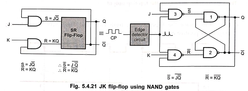
In the previous section we have seen the operation of JK flip–flop using SR
flip–flop and AND gates. It is not necessary to use the AND gates of Fig.
5.4.19 (a), since the same function can be performed by adding an extra input
terminal to NAND gates 3 and 4 of Fig. 5.4.21. Fig. 5.4.21 shows the modified
circuit of JK flip–flop which has only NAND gates.
2. Race–around Condition
•
In JK flip–flop, when J = K = 1, the output toggles (output changes either from
0 to 1 or from 1 to 0). Consider that initially Q = 0 and J = K = 1. After a
time interval ∆t equal to the propagation delay through two NAND gates in
series, the output will change to Q = 1 and after another time interval of ∆t
the output will change back to Q = 0. This toggling will continue until the
flip–flop is enabled and J = K = 1. At the end of clock pulse the flip–flop is
disabled and the value of Q is uncertain. This situation is referred to as the race–around condition. This is
illustrated in Fig. 5.4.22. This condition exists when tp ≥ ∆t. Thus
by keeping tp< ∆t we can avoid race around condition.
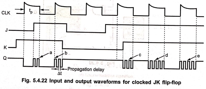
We
can keep tp < ∆t by keeping the duration of edge less than ∆t. A
more practical method for overcoming this difficulty is the use of the Master–Slave
(MS) configuration.
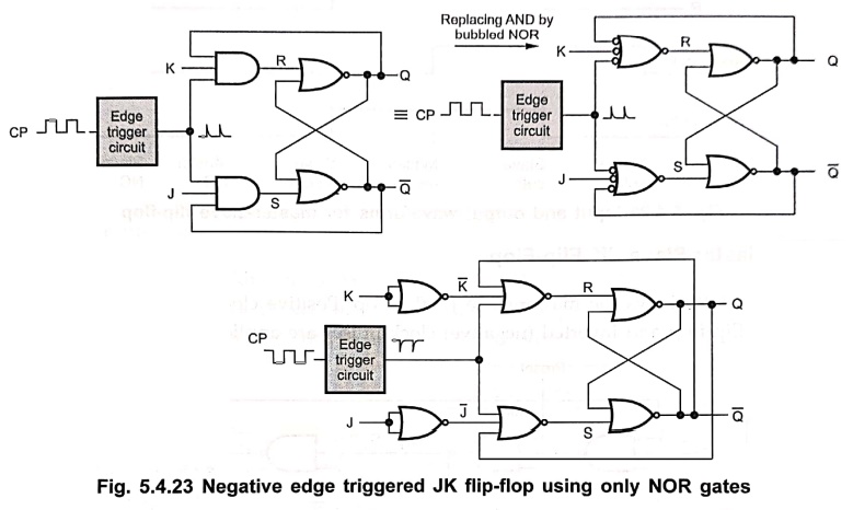
Example: 4
Realize a JK flip–flop
using only NOR gates.
Solution :
6. Master–Slave SR Flip–Flop
•
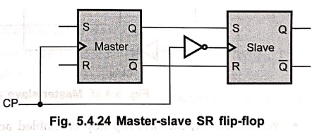
A master–slave flip–flop is constructed from two flip–flops. One circuit serves
as a master and the other as a slave, and the overall circuit is referred to as
a master–slave flip–flop. Fig. 5.4.24 shows SR master–slave flip–flop. It
consists of a master flip–flop, a slave flip–flop, and an inverter. Both the
flip–flops are positive level triggered, but inverter connected at the clock
input of the slave flip–flop forces it to trigger at the negative level.
•
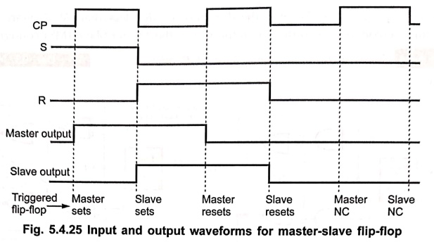
The output state of the master flip–flop is determined by the S and R inputs at
the positive clock pulse. The output state of the master is then transferred as
an input to the slave flip–flop. The slave flip–flop uses this input at the
negative clock pulse to determine its output state. Fig. 5.4.25 illustrates the
operation of the master–slave flip–flop.
7. Master–Slave JK Flip–Flop
•
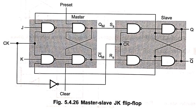
Fig. 5.4.26 shows the master–slave JK flip–flop. Positive clock pulses are
applied to first flip–flop and inverted (negative) clock pulses are applied to
second flip–flop.
•
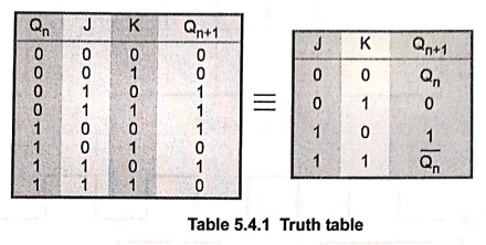
When CK = 1, the first flip–flop is enabled and the outputs QM and  responds to the inputs of J and K according to Table 5.4.1. At
this time, the second flip–flop is inhibited because its clock is low,
responds to the inputs of J and K according to Table 5.4.1. At
this time, the second flip–flop is inhibited because its clock is low,  = 0.
= 0.
•
When CK goes Low ( = 1), the first flip–flop is inhibited and
second flip–flop is enabled. At this time, the output of second flip–flop (Q
and ) follow the outputs QM and ,
respectively.
•
Since the second flip–flop follows the first one, it is referred to as the slave and the first one as the master.
•
In master–slave JK flip–flop state change occurs when flip–flop goes through
both positive transition (first half) of clock and negative transition of the
clock (second half). Thus, race–around condition does not exist in the master–slave
JK flip–flop.
8. T Flip–Flop
•
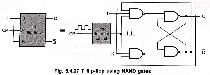
T flip–flop is also known as "Toggle
flip–flop'. The T flip–flop is a modification of the JK flip–flop. As shown
in Fig. 5.4.27, the T flip–flop is obtained from a JK flip–flop by connecting
both inputs, J and K together.
•
When T = 0, J = K = 0 and hence there is no change in the output. When T = 1, J
= K = 1 and hence output toggles.
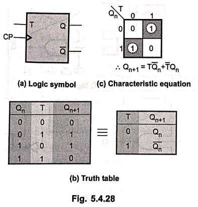
Fig.
5.4.28 shows logic symbol, truth table and the characteristic equation for T
flip–flop.
(a) Logic symbol, (b) Truth table, (c) Characteristic equation
Example: 5
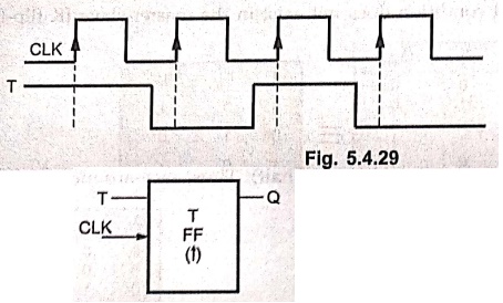
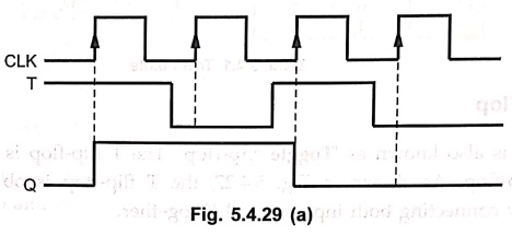
Refer Fig. 5.4.29 and
determine the Q output waveform if the flip–flop starts out RESET.
Solution :
9. Asynchronous or Direct Inputs
•
For the flip–flops discussed so far, the SR, D, JK, and T, the inputs are
called synchronous inputs because data on these inputs are transferred to the
flip–flop's output only on the triggering edge of the clock pulse; that is, the
data are transferred synchronously with the clock.
•
When power is turn ON, the state of
the flip–flop is uncertain. It may come to set (Q = 1) or reset (Q = 0) state.
In many applications, it is necessary to initially set or reset the flip–flop.
Such initial state of flip–flop can be accomplished by using the direct or
asynchronous inputs of the flip–flop. These inputs are :  and
and  They can be applied at any time between clock
pulses and are not in synchronism with the clock.
They can be applied at any time between clock
pulses and are not in synchronism with the clock.
•
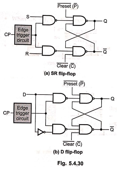
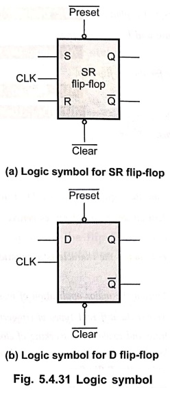
Fig. 5.4.30 shows the SR and D flip–flops with preset and clear inputs. These
are active–low inputs and thus when  =
=  = 1, the circuit
operates in accordance with the truth table of SR flip–flop. If = 1, and = 0, the flip–flop is reset and = 0 and =1, the flip–flop is set.
= 1, the circuit
operates in accordance with the truth table of SR flip–flop. If = 1, and = 0, the flip–flop is reset and = 0 and =1, the flip–flop is set.
Note :
Condition = = 0 must not be used, since this leads to an
uncertain state.
(b) Logic symbol for D
flip–flop
(a) Logic symbol for SR
flip–flop
Review Questions
1. Explain the working
of a master–slave JK flip–flop.
2. Realize a SR flip–flop
using NAND gates and explain its operation.
3. Derive the
characteristic equation of a SR flip–flop.
4. With reference to a
JK flip–flop, what is racing?
5. Differentiate
between flip–flop and latch.
6. Describe the input
and output action of JK master/slave flip–flops.
7. Draw the circuit
for SR flip–flop.
8. Realize SR flip–flop
using NOR gates and explain its operation.
9. Draw RS flipflop
circuit and explain its operation with truth table and suggest how to eliminate
the undetermined stage? Write some RS flipflop applications.
10. Explain the
operation of JK master slave flip–flop with suitable diagrams.
11. What is the
drawback of SR flip–flop? How is this minimized?
12. Explain the
working of JK flip–flop.
13. What is race
around condition and how is it overcome? Explain these concepts with relevant
timing diagrams.
14. Draw the clocked
RS flip–flop and explain with truth table.
15. How does a JK flip–flop
differ from the SR flip–flop in its basic operation?
16. Draw the logic
symbol and truth table of a D flip–flop.
17. Derive the
characteristic equation of a D flip flop.
18. Draw the logic
circuit of a clocked JK flip–flop.
19. Draw the logic
diagram of a D–FF using NAND gates and explain.
20. Mention any two
differences between the edge triggering and level triggering.
21. Write down the
characteristic equation and truth table for the JK flip–flop.
22. Mention the major
application of master slave flip–flop.
23. Explain the
different types of triggering with waveforms.
24. Draw and explain
the working of clocked D flip–flop.
25. How can race
condition be avoided in flip–flop ?
26. Explain the T flip–flop.
27. Explain the
operation of master–slave SR flip–flop.
28. Explain the use of
asynchronous inputs.
29. Draw the block
diagram of SR–FF and explain.
30. Explain the
operation of JK flip–flop with neat diagram.
Digital Principles and Computer Organization: Chapter 5: Sequential Circuits - Flip-Flops : Tag: : - Flip-Flops
Digital Principles and Computer Organization: Chapter 5: Sequential Circuits - Flip-Flops
Under Subject

Digital Principles and Computer Organization
CS25C06 2nd Semester AIDS, CSE, IT, CSE(CY) Dept | 2025 Regulation | 2nd Semester 2025 Regulation
Related Subjects

English Essentials II
EN25C02 2nd Semester | 2025 Regulation | 2nd Semester 2025 Regulation

Tamils and Technology தமிழர்களும் தொழில்நுட்பமும்
UC25H02 2nd Semester | 2025 Regulation | 2nd Semester 2025 Regulation

Linear Algebra
MA25C02 2nd Semester | 2025 Regulation

Applied Physics (CSIE) II
PH25C03 2nd Semester AIDS, CSE, IT, CSE(CY) Dept | 2025 Regulation | 2nd Semester 2025 Regulation
Digital Principles and Computer Organization
CS25C06 2nd Semester AIDS, CSE, IT, CSE(CY) Dept | 2025 Regulation | 2nd Semester 2025 Regulation

Basic Electrical and Electronics Engineering
EE25C01 2nd Semester | 2025 Regulation | 2nd Semester 2025 Regulation

Python for Data Science
AD25201 2nd Semester AIDS Dept | 2025 Regulation | 2nd Semester 2025 Regulation

Re-Engineering for Innovation
ME25C05 2nd Semester | 2025 Regulation | 2nd Semester 2025 Regulation

Python for Data Science - Laboratory
AD25201 2nd Semester AIDS Dept | 2025 Regulation | 2nd Semester 2025 Regulation