Digital Principles and Computer Organization: Chapter 5: Sequential Circuits - Flip-Flops
Sequential Circuits - Flip-Flops: Two Marks Important Questions and Answers
Digital Principles and Computer Organization
Digital Principles and Computer Organization: Chapter 5: Sequential Circuits - Flip-Flops: Anna University Part A Two Marks Important Questions and Answers
Digital Principles and Computer Organization:
Chapter 5: Sequential Circuits - Flip-Flops
Two Marks Questions
with Answers
1. What
is sequential circuit ?
Answer: Sequential circuit is
a broad category of digital circuit whose logic states depend on a specified
time sequence. A sequential circuit consists of a combinational circuit to
which memory elements are connected to form a feedback path.
2. What
are the classification of sequential circuits ?
Answer: The sequential
circuits are classified on the basis of timing of their signals into two types.
They are,
1)
Synchronous sequential circuit.
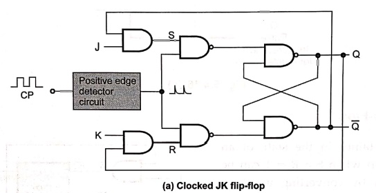
2)
Asynchronous sequential circuit.
3. What
is synchronous sequential circuit ?
Answer: A synchronous
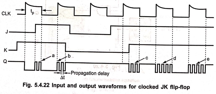
sequential circuit is a system whose behaviour can be defined from the
knowledge of its signal at discrete instants of time.
4. Give
the comparison between combinational circuits and sequential circuits.
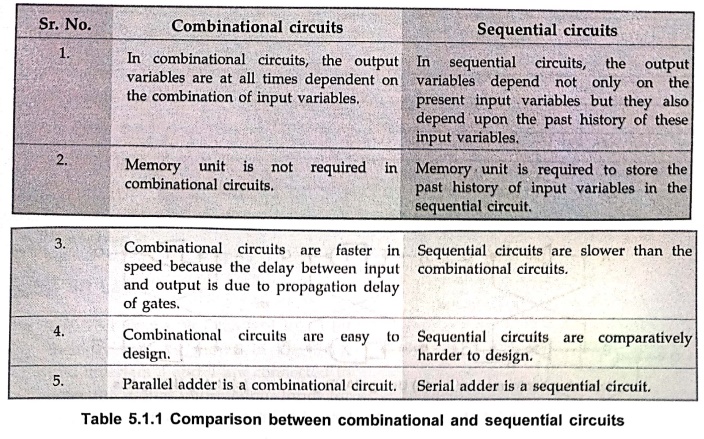
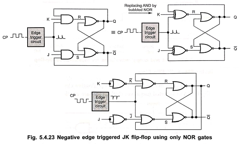
Combinational circuits
1.
In combinational circuits, the output variables are at all times dependent on
the combination of input variables.
2.
Memory unit is not required in combinational circuits.
3.
Combinational circuits are faster in speed because the delay between input and
output is due to propagation delay of gates.
4.
Combinational circuits are easy to design.
5.
Parallel adder is a combinational circuit.
Sequential
circuits
1.
In sequential circuits, the output variables depend not only on the present
input variables but they also depend upon the past history of these input
variables.
2.
Memory unit is required to store the past history of input variables in the
sequential circuit.
3.
Sequential Circuits are slower than the combinational circuits.
4.
Sequential circuits are comparatively harder to design.
5.
Serial adder is a sequential circuit.
5. Define
clock cycle.
The
time required to complete one cycle is called 'clock period' or 'clock
cycle'. Ideally, the clock signal should have sharp transitions from one
level to other.
6. Define
latch.
Answer: Latch is a simple memory element, which
consists of a pair of logic gates with their inputs and outputs inter connected
in a feedback arrangement, which permits a single bit to be stored.
7. What
do you mean by one–bit memory cell ?
If
the circuit is in the set (1) state, it will remain in the set state and if the
circuit is in the reset (0) state, it will remain in the reset state. This
property of the circuit shows that it can store 1–bit of digital information.
Therefore, the circuit is called a 1–bit
memory cell.
8. Draw
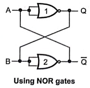
the NOR gate latch.
9. State
the disadvantages of SR latch.
An
SR (Set-Reset) latch is a fundamental bistable circuit used to store a single
bit of memory, but it has several critical drawbacks in digital logic design:
Undefined / Invalid
State: When both inputs are active at the same time (S = 1
and R = 1 for an NOR-based latch, or S = 0$ and R = 0 for a NAND-based latch),
both outputs (Q and  ) are forced to the same logic level. This
violates the rule that Q and must always be complements.
) are forced to the same logic level. This
violates the rule that Q and must always be complements.
Race Condition
(Metastability): If both inputs transition from the
invalid active state back to the inactive state simultaneously, the output
becomes unpredictable. The circuit enters a race condition where propagation
delays determine which state it settles into, often causing metastability.
No Clock Control (Level
Sensitive): Standard SR latches do not use a clock
signal. The output immediately responds to any change on the input pins, making
them susceptible to noise, glitches, and unwanted state changes whenever inputs
fluctuate.
Risk of Glitches:
High-frequency noise or momentary spikes on the input lines can unintentionally
set or reset the latch, leading to data corruption in sensitive systems.
Asynchronous Operation:
Because inputs affect the output directly without central synchronization,
integrating basic SR latches into complex synchronous digital systems (like
CPUs or timed microcontrollers) is difficult.
These
design limitations are why standard SR latches are rarely used in complex
digital systems and are typically upgraded to Gated SR latches, JK flip-flops
(which eliminate the invalid state), or D flip-flops (which ensure synchronous,
controlled data storage).
10. Give
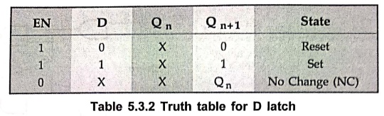
the truth table of transparent latch.
11. Draw
D–latch with truth table.
12. Define
flip–flop.
Answer: The basic unit for storage is flip–flop. A
flip–flop maintains its output state either at 1 or 0 until directed by an
input signal to change its state.
13. What
are the different types of flip–flop ?
Answer: There are various
types of flip–flops. Some of them are mentioned below they are,
•
RS flip–flop
•
SR flip–flops
•
D flip–flop
•
JK flip–flop
•
T flip–flop
14. Draw
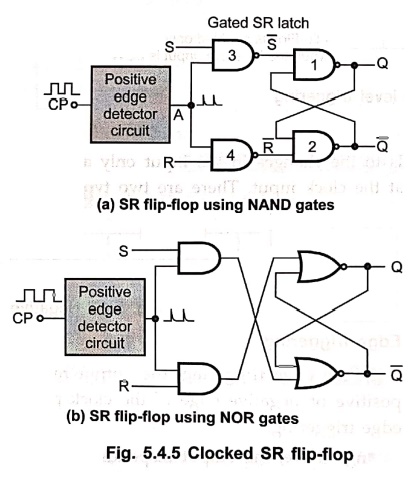
the circuit of SR flip–flop.
15. With
reference to a JK flip–flop, what is racing ?
Answer: In a level triggered J–K
flip–flop, when J and K are both high, then the output toggles continuously.
This condition is called a race around condition.
16.
Differentiate between flip–flop and latch.
Ans :
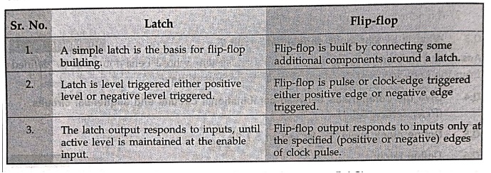
Latch
1.
A simple latch is the basis for flip–flop building.
2.
Latch is level triggered either positive level or negative level triggered.
3.
The latch output responds to inputs, until active level is maintained at the
enable input.
Flip–flop
1.
Flip–flop is built by connecting some additional components around a latch.
2.
Flip–flop is pulse or clock–edge triggered either positive edge or negative
edge triggered.
3.
Flip–flop output responds to inputs only at the specified (positive or
negative) edges of clock pulse.
17. What
is the operation of SR flip–flop ?
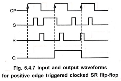
Case 1: If
S = R = 0 and the clock pulse is
applied, the output do not change, i.e. Qn + 1 = Qn. This
is indicated in the first row of the truth table.
Case 2 :
If S = 0, R = 1 and the clock pulse is
applied, Qn + 1 = 0. This is indicated in the second row of the
truth table.
Case 3 :
If S = 1, R = 0 and the clock pulse is applied, Qn + 1 = 1. This is
indicated in the third row of the truth table.
Case 4 : If
S = R = 1 and the clock pulse is applied, the state of the flip–flip is
undefined and therefore is indicated as indeterminate in the fourth row of the
truth table.
18. What
is the operation of D flip–flop ?
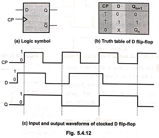
Answer: In D flip–flop during the occurrence of clock
pulse if D = 1, the output Q is set and if D = 0, the output is reset.
19. What
is the operation of JK flip–flop ?
Answer:
•
When K input is low and J input is high the Q output of flip–flop is set.
•
When K input is high and J input is low the Q output of flip–flop is reset.
•
When both the inputs K and J are low the output does not change.
•
When both the inputs K and J are high the output toggle on the next positive
clock edge.
20. What
is drawback of SR F–F ? How is this minimized?
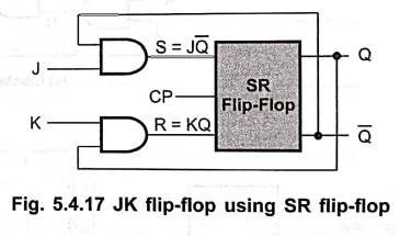
The uncertainty in the state of an SR flip–flop when S= R = 1 can be eliminated by converting it into a JK flip–flop. The data inputs are J and K which are ANDed with Q and Q, respectively, to obtain S and R inputs, as shown in Fig. 5.4.17. Thus, S = J. and R = K .Q.
21. How
does a JK F–F differ from SR F–F in its basic operation ?
The SRFF circuit is similar to SR latch except enable signal is replaced by the Clock Pulse (CP) followed by the positive edge detector circuit. The uncertainty in the state of an SR flip–flop when S= R = 1 can be eliminated by converting it into a JK flip–flop. The data inputs are J and K which are ANDed with Q and Q, respectively, to obtain S and R inputs, as shown in Fig. 5.4.17. Thus, S = J. and R = K .Q.
22. Draw
the logic symbol, truth table and waveform of D F–F.
23. What
is the operation of T flip–flop ?
Answer: T flip–flop is also
known as Toggle flip–flop.
•
When T = 0 there is no change in the output.
•
When T = 1 the output switch to the complement state (i.e.) the output toggles.
24. What
is a master–slave flip–flop ?
Answer: A master–slave flip–flop
consists of two flip–flops where one circuit serves as a master and the other
as a slave. The output of the master flip–flop is fed as an input to the slave
flip–flop. The master flip–flop is triggered at the positive edge of the clock
and slave flip–flop is triggered at the negative edge of the clock.
25. Differentiate between edge triggering and level triggering.
Level triggering:
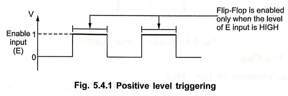
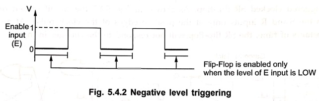
• In the level triggering, the output state is allowed to change according to input(s) when active level (either positive or negative) is maintained at the enable input. There are two types of level triggered latches :
• Positive level triggered : The output of flip–flop responds to the input changes only when its enable input is 1 (HIGH).
• Negative level triggered : The output of flip–flop responds to the input changes only when its enable input is 0 (LOW).
Edge triggering:
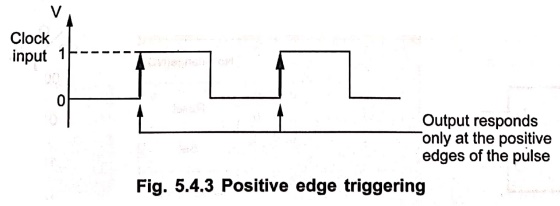
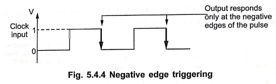
In the edge triggering, the output responds to the changes in the input only at the positive or negative edge of the clock pulse at the clock input. There are two types of edge triggering.
• Positive edge triggering : Here, the output responds to the changes in the input only at the positive edge of the clock pulse at the clock input.
• Negative edge triggering : Here, the output responds to the changes in the input only at the negative edge of the clock pulse at the clock input.
26. Define
race around condition.
In
JK flip–flop, when J = K = 1, the output toggles (output changes either from 0
to 1 or from 1 to 0). Consider that initially Q = 0 and J = K = 1. After a time
interval ∆t equal to the propagation delay through two NAND gates in series,
the output will change to Q = 1 and after another time interval of ∆t the
output will change back to Q = 0. This toggling will continue until the flip–flop
is enabled and J = K = 1. At the end of clock pulse the flip–flop is disabled
and the value of Q is uncertain. This situation is referred to as the race–around condition.
27. What
is edge–triggered flip–flop ?
Answer: The problem of race
around condition can solved by edge triggering flip flop. The term edge
triggering means that the flip–flop changes state either at the positive edge
or negative edge of the clock pulse and it is sensitive to its inputs only at
this transition of the clock.
28. What
is a master–slave flip–flop ?
(Refer section 5.4.7)
29. What
do you mean by triggering of flip–flop ?
Answer: The state of a flip–flop
is switched by a momentary change in the input signal. This momentary change is
called a trigger and the transition it causes is said to trigger the flip–flop.
30.
Realize JK flip–flops.
31. Draw
the logic circuit of a clocked JK flip–flop.
32. Define race around condition in flip flop.
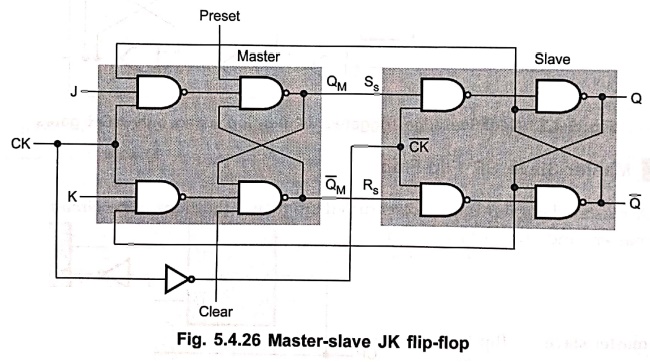
Fig.
5.4.26 shows the master–slave JK flip–flop. Positive clock pulses are applied
to first flip–flop and inverted (negative) clock pulses are applied to second
flip–flop.
•
When CK = 1, the first flip–flop is enabled and the outputs QM and  responds to the inputs of J and K according to Table 5.4.1. At
this time, the second flip–flop is inhibited because its clock is low,
responds to the inputs of J and K according to Table 5.4.1. At
this time, the second flip–flop is inhibited because its clock is low,  = 0.
= 0.
33. Derive
the characteristic equation of D flip–flop.
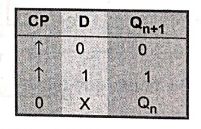
Looking at the truth table for D flip–flop we can realize that Qn+1 function follows D input at the positive going edges of the clock pulses. Hence the characteristic equation for D flip–flop is Qn+1 = D. However, the output Qn+1 is delayed by one clock period. Thus, D flip–flop is also known as delay flip–flop.
34. Give
the excitation table for JK flip–flop.
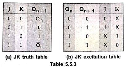
35.
Obtain the excitation table of D and JK flip–flops.
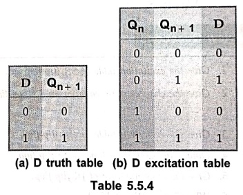
36. If
the input frequency of a T FF is 1600 kHz, TFF be the output frequency? Give
reason for your answer.
Answer: 800 kHz, because it
toggles at every clock pulse.
37. Draw state diagram of SR flip–flop.
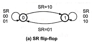
38. Give
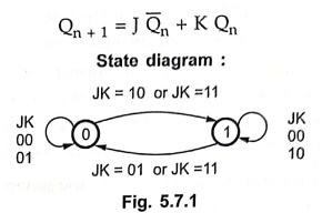
the characteristic equation and state diagram of JK flip–flop.
Answer:
• Characteristic
equation :
39. What is an excitation table ?
During the design process we know, from the transition table, the sequence of states, i.e., the transition from each present state to its corresponding next state. From this information we wish to find the flip–flop input conditions that will cause the required transition. For this reason, we need a table that lists the required inputs for a given change of state. Such a table is known as an excitation table of the flip–flop.
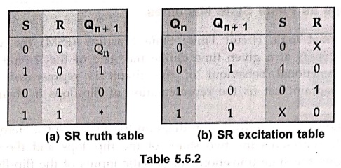
40. Give the excitation table of SR flip–flop.
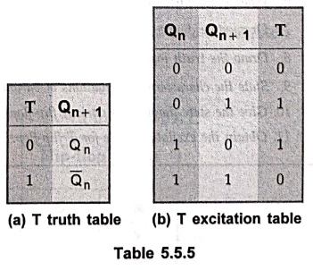
41. Give the excitation table of a T flip–flop
42. What
is a characteristic table ?
Answer: A characteristic table
defines the logical property of the flip–flop and completely characteristic its
operation
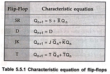
43. Give the characteristic equation of a SR flip–flop.
44. Give the characteristic equation of a D flip–flop.
45. Give the characteristic equation of a JK flip–flop.
46. Give the characteristic equation of a T flip–flop.
47. What
is the difference between truth table and excitation table.
Answer:
i)
An excitation table is a table that lists the required inputs for a given
change of state.
ii)
A truth table is a table indicating the output of a logic circuit for various
input states.
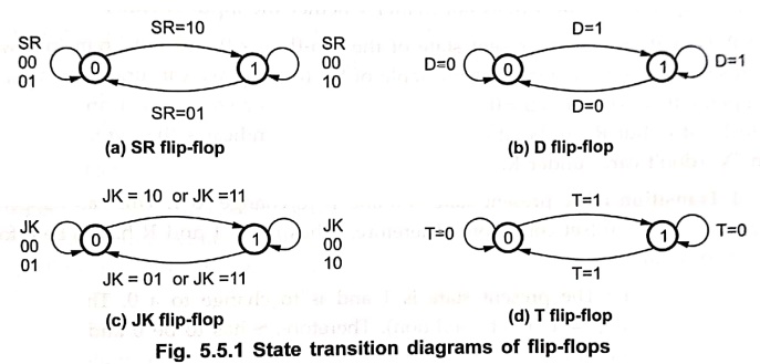
48. Draw
the state diagram of 'T' FF, 'D' FF.
49. Explain the flip–flop excitation tables for SR FF.
50. Explain the flip–flop excitation tables for T flip–flop.
51.
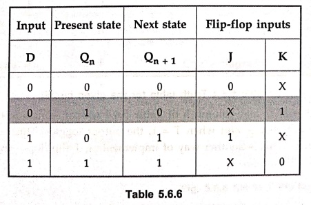
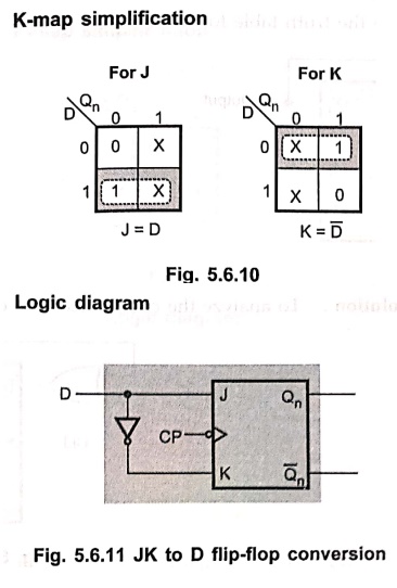
Convert JK FF to D FF.
The excitation table for above conversion is as shown in Table 5.6.6.
K–map simplification & Logic diagram
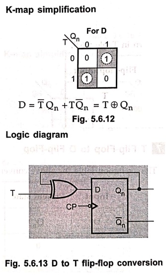
52.
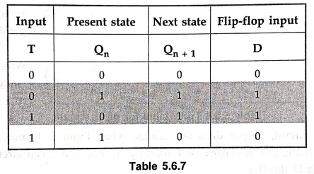
Convert D flip–flop to T flip–flop.
The excitation table for above conversion is as shown in Table 5.6.7.
K–map simplification & Logic diagram
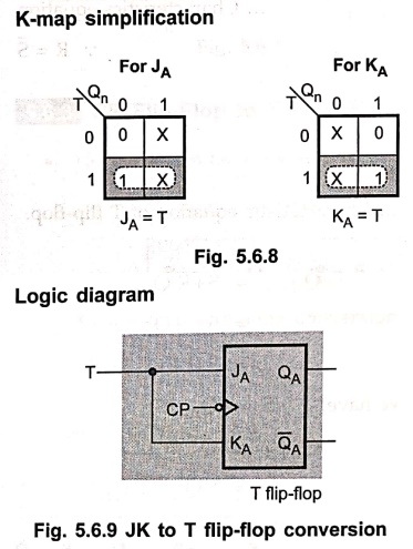
53. Convert JK flip–flop to T flip–flop.
The excitation table for above conversion is as shown in Table 5.6.5.
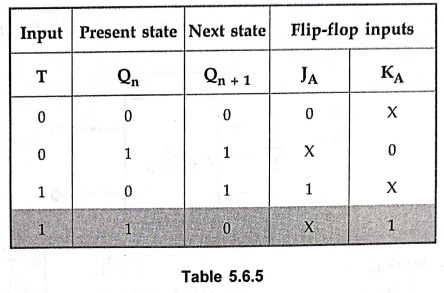
Logic diagram & K–map simplification
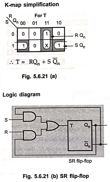
54. Convert a T F–F into SR F–F. Draw the circuit.
The excitation table for conversion of T FF into an SR FF is as shown in the table.
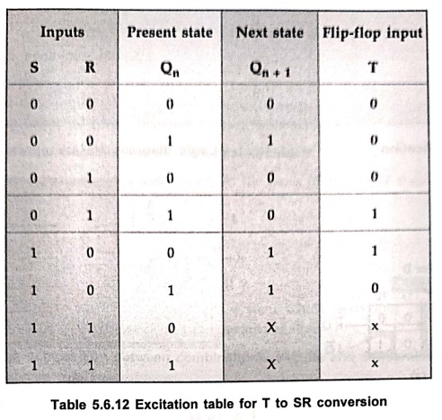
K–map simplification & Logic diagram
Digital Principles and Computer Organization: Chapter 5: Sequential Circuits - Flip-Flops : Tag: : Digital Principles and Computer Organization - Sequential Circuits - Flip-Flops: Two Marks Important Questions and Answers
Digital Principles and Computer Organization: Chapter 5: Sequential Circuits - Flip-Flops
Under Subject

Digital Principles and Computer Organization
CS25C06 2nd Semester AIDS, CSE, IT, CSE(CY) Dept | 2025 Regulation | 2nd Semester 2025 Regulation
Related Subjects

English Essentials II
EN25C02 2nd Semester | 2025 Regulation | 2nd Semester 2025 Regulation

Tamils and Technology தமிழர்களும் தொழில்நுட்பமும்
UC25H02 2nd Semester | 2025 Regulation | 2nd Semester 2025 Regulation

Linear Algebra
MA25C02 2nd Semester | 2025 Regulation

Applied Physics (CSIE) II
PH25C03 2nd Semester AIDS, CSE, IT, CSE(CY) Dept | 2025 Regulation | 2nd Semester 2025 Regulation
Digital Principles and Computer Organization
CS25C06 2nd Semester AIDS, CSE, IT, CSE(CY) Dept | 2025 Regulation | 2nd Semester 2025 Regulation

Basic Electrical and Electronics Engineering
EE25C01 2nd Semester | 2025 Regulation | 2nd Semester 2025 Regulation

Python for Data Science
AD25201 2nd Semester AIDS Dept | 2025 Regulation | 2nd Semester 2025 Regulation

Re-Engineering for Innovation
ME25C05 2nd Semester | 2025 Regulation | 2nd Semester 2025 Regulation

Python for Data Science - Laboratory
AD25201 2nd Semester AIDS Dept | 2025 Regulation | 2nd Semester 2025 Regulation