Digital Principles and Computer Organization: Chapter 5: Sequential Circuits - Flip-Flops
Various Representation of Flip-Flops
Questions: 1. Give the excitation table of SR flip-flop. 2. Give the characteristic equation and state diagram of JK flip-flop. 3. Give the excitation table for JK flip-flop. 4. Obtain the excitation table of D flip-flop. 5. Give the state diagram of JK flip-flop. 6. What is excitation table? 7. Draw state diagram of SR flip-flop. 8. Draw the truth table and excitation table of T flip-flop. 9. State the characteristics equations of various flip-flops. 10. Give the state diagram of various flip-flops. 11. Obtain the excitation table for T flip-flop.
Various Representation
of Flip–Flops
1. Characteristic Equations of Flip–Flops
•
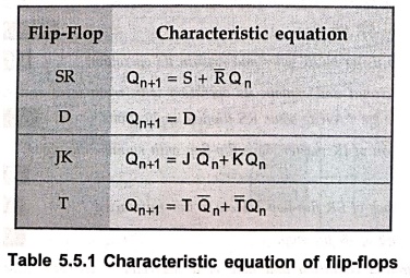
The characteristic equations for various flip–flops are summarized in Table
5.5.1.
2. Flip–Flops as Finite State Machines
•
In a sequential logic circuit Finite State Machine (FSM) the value of all the
memory elements at a given time define the state of that circuit at that time.
In FSM, the functional behaviour of the circuit is represented using the state
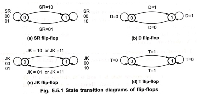
transition diagram. Let us the representation of flip–flops in their state
transition diagrams.
Fig.
5.5.1 shows the state transition diagram for all flip–flops. Here, the 0 and
the 1 in the circle represents the two states of the flip–flops and the arcs
with arrow heads indicate the state transitions for specific inputs of the flip–flop.
For example, when SR flip–flop is in state 0, it goes to state 1 if SR inputs
are 10, i.e. S = 1 and R = 0.
3. Flip–Flop Excitation Table
•
During the design process we know, from the transition table, the sequence of
states, i.e., the transition from each present state to its corresponding next
state. From this information we wish to find the flip–flop input conditions
that will cause the required transition. For this reason, we need a table that
lists the required inputs for a given change of state. Such a table is known as
an excitation table of the flip–flop.
•
We can derive the excitation tables for flip–flops from their truth tables. The
excitation table consists of two columns Qn and Qn+1, and
a column for each input to show how the required transition can be achieved.
Let us see the truth tables and excitation tables for SR, JK, D and T flip–flops.
1. SR Flip–Flop
•
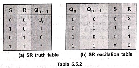
Table 5.5.2 (a) and (b) show the truth table and excitation tables for SR flip–flop,
respectively. As shown in the table, there are four possible transitions from
the present state to the next state. For each transition, the required input
condition is derived from the information available in the truth table. Let us see
the process by examining each case.
(a) SR truth table, (b) SR excitation table
Note :
The symbol "X" in the table represents a don't care condition, i.e.,
it indicates that to get required output it does not matter whether the input
is either 1 or 0.
0 → 0 Transition :
The present state of the flip–flop is 0 and is to remain 0 when a clock pulse
is applied. Looking at truth table of SR flip–flop we can understand that, this
can happen either when R = S = 0 (no–change condition) or when R = 1 and S = 0.
Thus, S has to be at 0, but R can be at either level. The table indicates this
with a "0" under S and an "X" (don't care) under R.
0 → 1 Transition :
The present state is 0 and is to change to 1. This can happen only when S = 1
and R = 0 (set condition). Therefore, S has to be 1 and R has to be 0 for this
transition to occur.
1→ 0 Transition :
The present state is 1 and is to change to a 0. This can happen only when S = 0
and R = 1 (reset condition). Therefore, S has to be 0 and R has to be 1 for
this transition to occur.
1 → 1 Transition :
The present state is 1 and is to remain 1. This can happen either when S = 1
and R = 0 (set condition) or when S = 0 and R = 0 (no change condition). Thus R
has to be 0, but S can be at either level. The table indicates this with a
"X" under S and "0" under R.
2. JK Flip–Flop
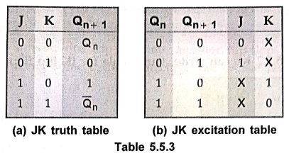
• The truth table and excitation table
for JK flip–flop are shown in Table 5.5.3 (a) and (b) respectively. Let us
examine each case.
0 → 0 Transition :
When both present state and next state are 0, the J input must remain at 0 and
the K input can be either 0 and 1.
0 → 1 Transition :
The present state is 0 and is to change to 1. This can happen either when J = 1
and K = 0 (set condition) or when J = K = 1 (toggle condition). Thus, J has to
be 1, but K can be at either level for this transition to occur.
1→ 0 Transition :
The present state is 1 and is to This can happen either when J = 0 and K = 1 or
when J = K = 1. Thus, K has to be 1 but J can be at either level.
(a) JK truth table, (b) JK excitation table
1→ 1 Transition : When
both present state and next are 1, the K input must remain at 0 while the J
input can be 0 or 1.
•
As seen from Table 5.5.3, the excitation table for JK flip–flop has more don't
care conditions than the excitation table for RS flip–flop. The don't care
terms usually simplify the function. Therefore, the combinational circuits
using JK flip–flops for the input functions are likely to be simpler than those
using RS flip–flops.
3. D Flip–Flop
•
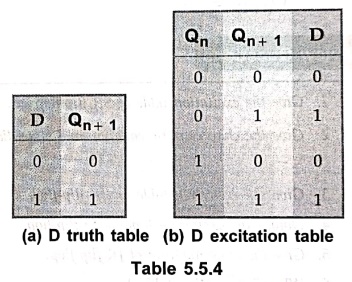
Table 5.5.4 (a) and (b) show the truth table and excitation table for D flip–flop,
respectively. In D flip–flop, the next state is always equal to the D input and
it is independent of the present state. Therefore, D must be 0 if Qn+1 has
to be 0, and 1 if Qn+ 1 has to be 1, regardless of the value of Qn.
4. T Flip–Flop
•
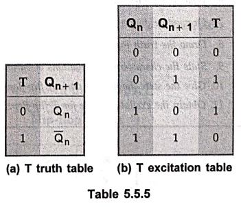
Table 5.5.5 (a) and (b) show the truth table and the excitation table for T
flip–flop, respectively. We know that when input T = 1, the state of the flip–flop
complemented; when T = 0, the state of the flip–flop remains unchanged.
Therefore, for 0 → 0 and 1 → 1 transitions T must be 0 and for 0 →1 and 1→ 0
transitions T must be 1.
(a) D truth table, (b) D excitation table
Example: 1
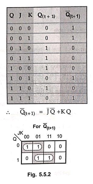
Show that the
characteristic equation of Q'(t+1) of JK flip–flop is Q'(t+1)
= J'Q'+KQ
Solution :
From
Fig. 5.5.2 we can write truth table for JK flip flop as shown below.
Review Questions
1. Give the excitation
table of SR flip–flop.
2. Give the
characteristic equation and state diagram of JK flip–flop.
3. Give the excitation
table for JK flip–flop.
4. Obtain the
excitation table of D flip–flop.
5. Give the state
diagram of JK flip–flop.
6. What is excitation
table?
7. Draw state diagram
of SR flip–flop.
8. Draw the truth
table and excitation table of T flip–flop.
9. State the
characteristics equations of various flip–flops.
10. Give the state
diagram of various flip–flops.
11. Obtain the
excitation table for T flip–flop.
Digital Principles and Computer Organization: Chapter 5: Sequential Circuits - Flip-Flops : Tag: : - Various Representation of Flip-Flops
Digital Principles and Computer Organization: Chapter 5: Sequential Circuits - Flip-Flops
Under Subject

Digital Principles and Computer Organization
CS25C06 2nd Semester AIDS, CSE, IT, CSE(CY) Dept | 2025 Regulation | 2nd Semester 2025 Regulation
Related Subjects

English Essentials II
EN25C02 2nd Semester | 2025 Regulation | 2nd Semester 2025 Regulation

Tamils and Technology தமிழர்களும் தொழில்நுட்பமும்
UC25H02 2nd Semester | 2025 Regulation | 2nd Semester 2025 Regulation

Linear Algebra
MA25C02 2nd Semester | 2025 Regulation

Applied Physics (CSIE) II
PH25C03 2nd Semester AIDS, CSE, IT, CSE(CY) Dept | 2025 Regulation | 2nd Semester 2025 Regulation
Digital Principles and Computer Organization
CS25C06 2nd Semester AIDS, CSE, IT, CSE(CY) Dept | 2025 Regulation | 2nd Semester 2025 Regulation

Basic Electrical and Electronics Engineering
EE25C01 2nd Semester | 2025 Regulation | 2nd Semester 2025 Regulation

Python for Data Science
AD25201 2nd Semester AIDS Dept | 2025 Regulation | 2nd Semester 2025 Regulation

Re-Engineering for Innovation
ME25C05 2nd Semester | 2025 Regulation | 2nd Semester 2025 Regulation

Python for Data Science - Laboratory
AD25201 2nd Semester AIDS Dept | 2025 Regulation | 2nd Semester 2025 Regulation