Digital Principles and Computer Organization: Chapter 5: Sequential Circuits - Flip-Flops
One-Bit Memory Cell
Sequential Circuits
Questions: 1. Explain the operation of one-bit memory cell. 2. Draw the NOR gate latch and write its truth table.
One–Bit Memory Cell
•
Fig. 5.2.1 shows the basic bistable element used in latches and flip–flops. The
basic bistable element has two outputs Q and  . It has two cross–coupled
inverters, i.e., the output of the first inverter is connected as an input to
the second inverter and the output of second inverter is connected as an input
to the first inverter.
. It has two cross–coupled
inverters, i.e., the output of the first inverter is connected as an input to
the second inverter and the output of second inverter is connected as an input
to the first inverter.
•
The basic bistable element circuit has two stable states logic 0 and logic 1,
hence the name 'bistable'. To illustrate this, assume A = 0. When A = 0, the
output of inverter 1 is 1 (Ā), i.e., Q = 1.
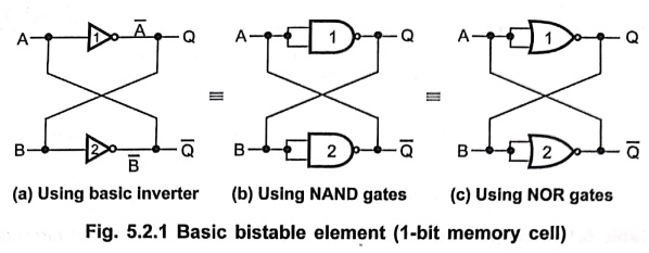
Since the output of inverter 1 is the input to the inverter
2, Ā = B = 1. Consequently, the output of inverter 2, i.e.,  is 0.
Since the output of the inverter 2 is connected to the input of the inverter 1, = = A = 0. We have assumed same value for A. Thus, the
circuit is stable with = A = = 0 and Q Ā = B = 1. Using
similar explanation it is easy to show that if it is assumed that A =1, the
basic bistable element is stable with = A = = 1 and Q
= Ā = B = 0. This is a second stable condition of the basic bistable element.
is 0.
Since the output of the inverter 2 is connected to the input of the inverter 1, = = A = 0. We have assumed same value for A. Thus, the
circuit is stable with = A = = 0 and Q Ā = B = 1. Using
similar explanation it is easy to show that if it is assumed that A =1, the
basic bistable element is stable with = A = = 1 and Q
= Ā = B = 0. This is a second stable condition of the basic bistable element.
•
The two stable states of basic bistable elements are used to store two binary
elements, 0 and 1. In positive logic system, state Q = 1 is used to store logic
1, and state Q = 0 is used to store logic 0. It is important to note that the
two outputs are complementary. That is when Q = 0, = 1; and
when = 1, = 0.
•
From the above discussion we can note following things about the basic bistable
element.
1.
The outputs Q and are always complementary.
2.
The circuit has two stable states. The state corresponds to Q = 1 is referred
to as 1 state or set state and state corresponds to Q = 0 is referred to as 0 state or Reset state.
3.
If the circuit is in the set (1) state, it will remain in the set state and if
the circuit is in the reset (0) state, it will remain in the reset state. This
property of the circuit shows that it can store 1–bit of digital information.
Therefore, the circuit is called a 1–bit
memory cell.
4.
The 1–bit information stored in the circuit is locked or latched in the
circuit. Therefore, this circuit is also referred to as a latch.
Review Questions
1. Explain the
operation of one–bit memory cell.
2. Draw the NOR gate
latch and write its truth table.
Digital Principles and Computer Organization: Chapter 5: Sequential Circuits - Flip-Flops : Tag: : Sequential Circuits - One-Bit Memory Cell
Digital Principles and Computer Organization: Chapter 5: Sequential Circuits - Flip-Flops
Under Subject

Digital Principles and Computer Organization
CS25C06 2nd Semester AIDS, CSE, IT, CSE(CY) Dept | 2025 Regulation | 2nd Semester 2025 Regulation
Related Subjects

English Essentials II
EN25C02 2nd Semester | 2025 Regulation | 2nd Semester 2025 Regulation

Tamils and Technology தமிழர்களும் தொழில்நுட்பமும்
UC25H02 2nd Semester | 2025 Regulation | 2nd Semester 2025 Regulation

Linear Algebra
MA25C02 2nd Semester | 2025 Regulation

Applied Physics (CSIE) II
PH25C03 2nd Semester AIDS, CSE, IT, CSE(CY) Dept | 2025 Regulation | 2nd Semester 2025 Regulation
Digital Principles and Computer Organization
CS25C06 2nd Semester AIDS, CSE, IT, CSE(CY) Dept | 2025 Regulation | 2nd Semester 2025 Regulation

Basic Electrical and Electronics Engineering
EE25C01 2nd Semester | 2025 Regulation | 2nd Semester 2025 Regulation

Python for Data Science
AD25201 2nd Semester AIDS Dept | 2025 Regulation | 2nd Semester 2025 Regulation

Re-Engineering for Innovation
ME25C05 2nd Semester | 2025 Regulation | 2nd Semester 2025 Regulation

Python for Data Science - Laboratory
AD25201 2nd Semester AIDS Dept | 2025 Regulation | 2nd Semester 2025 Regulation