Digital Principles and Computer Organization: Chapter 5: Sequential Circuits - Flip-Flops
Latches: SR, Gated SR, Gated D Latches
Questions: 1. What is SR latch? Explain it's operation. 2. What is gated SR latch? 3. Explain the working of gated D latch with truth table and characteristic equation.
Latches
1. SR Latch
•
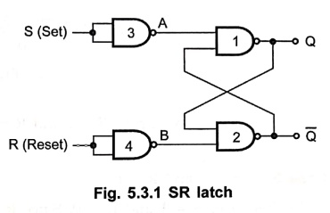
Fig. 5.3.1 shows SR latch which is 1–bit memory cell. As shown in Fig. 5.3.1,
two inverters 3 and 4 are connected to enter the digital information. Input for
gate 3 is S and input for gate 4 is R. This latch is also called RS latch.
•
For understanding the circuit operation, we must first determine the output of
NAND gate whose one of the input is logic 0 and accordingly we have to
determine the output of other NAND gate in the cross coupled circuit. Because
the output of NAND gate is 1 if any one input is 0. The circuit operation is as
follows. In Fig. 5.3.2, the output of shaded NAND gate is determined first, and
the 0 input that decides the output of shaded NAND as 1 is shown in bold.
Case 1 : S = R = 0
In
this case,  =
=  = 1. If Q is 1, Q and B inputs for NAND gate
2 are both 1 and hence output
= 1. If Q is 1, Q and B inputs for NAND gate
2 are both 1 and hence output  = 0. Since = 0 and = 1, the output of NAND gate 1 is 1, i.e. Q = 1.
If
Q is 0, Q and inputs for
NAND gate 2 are 0 and 1, and hence output = 1. Since = 1 and = 1, the output
of NAND gate 1 is 0, i.e., Q = 0.
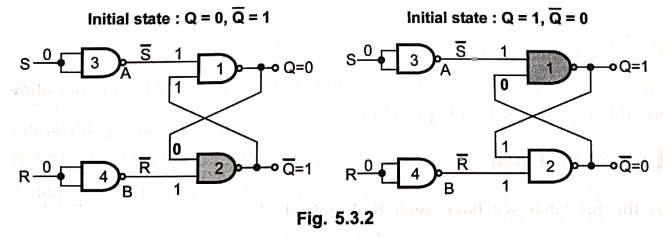
This shows that when S
= R = 0, the outputs do not change.
Case 2 : S = 1 and R =
0
In
this case, = 0 and =1. = 0, the output of NAND gate 1, Q = 1 (Recall that, for NAND
any one or more input is 0, the output is 1) For NAND gate 2, both inputs Q and are 1, thus output = 0.
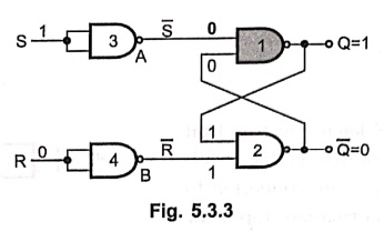
The inputs S = 1 and R
= 0, makes Q = 1, i.e., set state.
Case 3 : S = 0 and R =
1
In
this case, = 1 and = 0. Since = 0, the
output of NAND gate 2, = 1. For NAND gate 1, both inputs and are 1, thus output Q = 0.
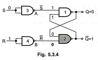
The inputs S = 0 and R
= 1, makes Q = 0, i.e., reset state.
Case 4 : S = 1 and R =
1
When
S = R = 1, both the outputs Q and try to become 1 which is not allowed
and therefore, this input condition is prohibited.
2. Gated SR Latch
•
In the SR latch we have seen that output changes occur immediately after the
input changes occur i.e. the latch is sensitive to its S and R inputs at all
times. However, it can easily be modified to create a latch that is sensitive
to these inputs only when an enable input is active. Such a latch with enable
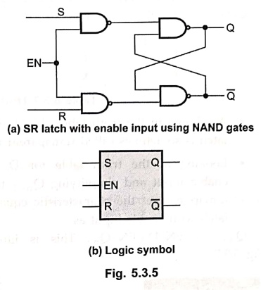
input is known as gated SR latch. It
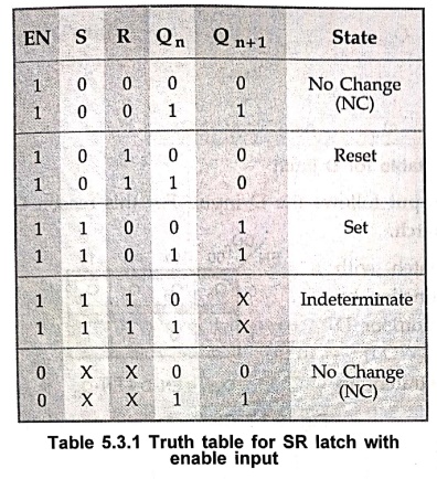
is as shown in Fig. 5.3.5. Table 5.3.1 shows the truth table for gated latch.
As shown by truth table, the circuit behaves like a SR latch when EN = te
previous state w 1, and retains its previous state when EN = 0.
3. Gated D Latch
•
Looking at the truth table of the SR latch we can realize that when both inputs
are same the output either does not change or it is invalid (Inputs → 00, no
change and inputs → 11, invalid). In many practical applications, these input conditions
are not required. These input conditions can be avoided by making them
complement of each other. This modified SR latch is known as D latch.
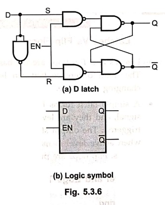
• Fig. 5.3.6 shows the D latch. The NAND gates 1, 2, 3 and 4 form the basic SR latch with enable input. The fifth NAND gate is level used to provide the complemented inputs.
•
As shown in Fig. Fig. 5.3.6, D input goes directly to the S input, and its
complement is applied to the R input, through gate 5. Therefore, only two input
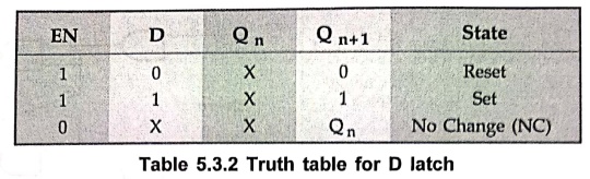
conditions exists, either S = 0 and R = 1 or S = 1 and R = 0. The truth table
for D (no latch is as shown in Table 5.3.2.
•
As shown in the truth table, the Q output follows the D input. For this reason
D latch is sometimes called transparent
latch.
•
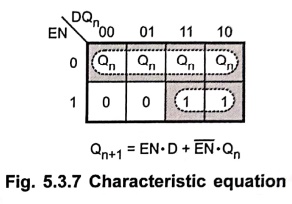
Looking at the truth table for D latch with enable input and simplifying Qn+1
function by k–map we get the characteristic equation for D latch with
enable input as
Qn+1
= EN.D+  .Qn . This is
illustrated in Fig .5.3.7.
.Qn . This is
illustrated in Fig .5.3.7.
Review Questions
1. What is SR latch?
Explain it's operation.
2. What is gated SR
latch?
3. Explain the working
of gated D latch with truth table and characteristic equation.
Digital Principles and Computer Organization: Chapter 5: Sequential Circuits - Flip-Flops : Tag: : - Latches: SR, Gated SR, Gated D Latches
Digital Principles and Computer Organization: Chapter 5: Sequential Circuits - Flip-Flops
Under Subject

Digital Principles and Computer Organization
CS25C06 2nd Semester AIDS, CSE, IT, CSE(CY) Dept | 2025 Regulation | 2nd Semester 2025 Regulation
Related Subjects

English Essentials II
EN25C02 2nd Semester | 2025 Regulation | 2nd Semester 2025 Regulation

Tamils and Technology தமிழர்களும் தொழில்நுட்பமும்
UC25H02 2nd Semester | 2025 Regulation | 2nd Semester 2025 Regulation

Linear Algebra
MA25C02 2nd Semester | 2025 Regulation

Applied Physics (CSIE) II
PH25C03 2nd Semester AIDS, CSE, IT, CSE(CY) Dept | 2025 Regulation | 2nd Semester 2025 Regulation
Digital Principles and Computer Organization
CS25C06 2nd Semester AIDS, CSE, IT, CSE(CY) Dept | 2025 Regulation | 2nd Semester 2025 Regulation

Basic Electrical and Electronics Engineering
EE25C01 2nd Semester | 2025 Regulation | 2nd Semester 2025 Regulation

Python for Data Science
AD25201 2nd Semester AIDS Dept | 2025 Regulation | 2nd Semester 2025 Regulation

Re-Engineering for Innovation
ME25C05 2nd Semester | 2025 Regulation | 2nd Semester 2025 Regulation

Python for Data Science - Laboratory
AD25201 2nd Semester AIDS Dept | 2025 Regulation | 2nd Semester 2025 Regulation