Digital Principles and Computer Organization: Chapter 11: Memory
Memory: Two Marks Important Questions and Answers
Digital Principles and Computer Organization
Digital Principles and Computer Organization: Chapter 11: Memory: Anna University Part A Two Marks Important Questions and Answers
Digital
Principles and Computer Organization:
Chapter 11: Memory
Two
Marks Questions with Answers
1. Name
the two types of storage devices.
Answer:
The
two types of storage devices are :
1.
Primary memory
2.
Secondary memory.
2. Define
memory latency.
Answer: The term memory
latency is used to refer to the amount of time it takes to transfer a word of
data to or from the memory. The term latency is used to denote the time it
takes to transfer the first word of data. This time is usually substantially
longer than the time needed to transfer each subsequent word of a block.
3. Define
memory bandwidth.
Answer: Memory bandwidth is a
product of the rate at which the data are transferred (and accessed) and the
width of the data bus.
4. What
will be the width of address and data buses for a 512 K × 8 memory chip?
Answer: The widths of address
and data buses are 19 and 8, respectively.
5. What
do you mean by memory hierarchy ?
Answer: A memory hierarchy is
a structure of memory that uses multiple levels of memories; as the distance
from the processor increases, the size of the memories and the access time both
increase.
6. What
is the need to implement memory as a hierarchy ?
Answer: Ideally, computer
memory should be fast, large and inexpensive. Unfortunately, it is impossible
to meet all the three of these requirements using one type of memory. Hence it
is necessary to implement memory as a hierarchy.
7. What
are registers in a computer system ?
Answer:
Registers
are the smallest and fastest memory
units located inside the CPU. They store data, instructions, and addresses
that the processor needs immediately during execution.
8. Why
are registers considered the fastest memory?
Answer: Registers are built
using high–speed circuits and work at the same clock speed as the CPU.
Therefore, they provide data to the processor much faster than cache or main
memory.
9. State
any two characteristics of registers.
Answer:
•
They are the fastest memory in the
hierarchy.
•
They are very small in size, usually
a few dozen or a few hundred.
10. Name
the two types of RAM.
Answer:
The
two types of RAM are :
1.
Static RAM
2.
Dynamic RAM
11. Distinguish
between static RAM and dynamic RAM.
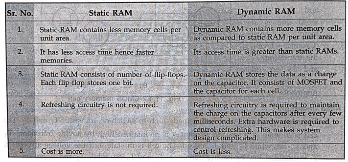
Static RAM
1.
Static RAM contains less memory cells per unit area.
2.
It has less access time hence faster memories.
3.
Static RAM consists of number of flip–flops. Each flip–flop stores one bit.
4.
Refreshing circuitry is not required.
5.
Cost is more.
Dynamic RAM
1.
Dynamic RAM contains more memory cells as compared to static RAM per unit area.
2.
Its access time is greater than static RAMs.
3.
Dynamic RAM stores the data as a charge on the capacitor. It consists of MOSFET
and the capacitor for each cell.
4.
Refreshing circuitry is required to maintain the charge on the capacitors after
every few milliseconds. Extra hardware is required to control refreshing. This
makes system design complicated.
5.
Cost is less.
12. What
are static memories ?
Answer: Memories that consists
of circuits capable of retaining their state as long as power is applied are
known as static memories.
13. What
are static and dynamic memories ?
Answer: Static memory are
memories which require periodic no refreshing. Dynamic memories are memories,
which require periodic refreshing.
14. Give
the features of a ROM cell.
Answer: The main features of a
ROM cell are :
•
It can hold one bit data.
•
It can hold data even if power is turned off.
•
We can not write data in ROM cell; it is read only.
15. Name
the different types of ROMs.
Answer: There are four types
of ROMs are :
1.
Masked ROM
2.
PROM
3.
EPROM and
4.
EEPROM or E2PROM.
16. What
is the function of memory controller ?
Answer: The memory controller
is connected between processor and the DRAM memory. It does the task of
generating multiplexed address as well as task of generating control signals
such as  and so on for DRAM.
17. What
is refreshing overhead ?
Answer:
Refreshing
overhead = Time required for refresh / Interval time
18. Compare
SDRAM with DDR SDRAM.
Answer: The standard SDRAM
performs its operations on the rising edge of the clock signal. On the other
hand, the DDR SDRAMs transfers data on both the edges of the clock signal. The
latency of the DDR SDRAMs is same as that for standard SDRAM. However, since
they transfer data on both the edges of the clock signal, their bandwidth is
effectively doubled for long burst transfer.
19. Define track and sectors on the disk.
Answer: Each disk surface is
divided into concentric circles, called tracks.
There are typically tens of thousands of tracks per surface. Each track is in
turn divided into sectors that contain the information; each track may have
thousands of sectors. Sectors are typically 512 to 4096 bytes in size.
20.
Define rotational latency or rotational delay.
Answer: Rotational latency or
rotational delay is the time required for the desired sector of a disk to
rotate under the read/write head; usually assumed to be half the rotation time.
21. How
do you construct a 8 M × 32 memory using 512 K × 8 memory chips?
Answer: By connecting four 512
× 8 chips in parallel we can expand the word size to 32 and such sixteen blocks
consisting of four memory chips we can construct 8 M × 32 memory.
22. What
are the characteristics of semiconductor RAM memories ?
Answer: They are available in
a wide range of speeds.
Their
cycle time range from 100 ns to less than 10 ns.
They
replaced the expensive magnetic core memories.
They
are used for implementing memories.
23. Why
SRAMS are said to be volatile ?
Answer: SRAMs are said to be
volatile because their contents are lost when power is interrupted.
24. What
are the characteristics of SRAMS ?
Answer:
1.
SRAMs are fast
2.
They are volatile
3.
They are of high cost
4.
Less density.
25. What
are the characteristics of DRAMs ?
Answer:
1.
Low cost
2.
High density
3.
Refresh circuitry is needed.
26.
Define refresh circuit.
Answer: Refresh circuit is a
circuit which ensures that the contents of a DRAM are maintained when each row
of cells are accessed periodically.
27. What
are asynchronous DRAMs ?
Answer: In asynchronous DRAMs,
the timing of the memory ng of the memory device is controlled asynchronously.
A specialized memory controller circuit provides the necessary control signals
RAS and CAS that govern the timing. The processor must take into account the
delay in the response of the memory. Such memories are asynchronous DRAMs.
28. What
are synchronous DRAMs ?
Answer:
Synchronous
DRAMs are those whose operation is directly synchronized with a clock signal.
29. Define
memory access time.
Answer: The time required to
access one word is called the memory access time. Or It is the time that
elapses between the initiation of an operation and the completion of that
operation.
30. Define
memory cycle time.
Answer: It is the minimum time
delay required between the initiation of two successive memory operations. That
is the time between two successive read operations.
31.
Define memory cell.
Answer: A memory cell is
capable of storing one bit of information. It is usually organized in the form
of an array.
32. What
is a word line?
Answer: In a memory cell, all
the cells of a row are connected to a common line called word line.
33. What
is double data rate SDRAMs ?
Answer: Double data rates
SDRAMs are those which can transfer data on both edges of the clock and their
bandwidth is essentially doubled for long burst transfers.
34. Define
ROM.
Answer: It is a non–volatile
and read only memory.
35. What
are the features of PROM?
Answer: They are :
1.
Programmed directly by the user
2.
Faster
3.
Less expensive
4.
More flexible.
36. Why
EPROM chips are mounted in packages that have transparent window ?
Answer: Since the erasure
requires dissipating the charges trapped in the transistors of memory cells.
This can be done by exposing the chip to UV light.
37. What
are the disadvantages of EPROM ?
Answer: The chip must be
physically removed from the circuit for reprogramming and its entire contents
are erased by the ultraviolet light.
38. What
are the advantages and disadvantages of using EEPROM ?
Answer: The advantages are
that EEPROMS do not have to be removed for erasure. Also it is possible to
erase the cell contents selectively. The only disadvantage is that different
voltages are needed for erasing, writing and reading the stored data.
39. Define
flash memory.
Answer: Flash memories are read/write memories. In
flash memories it is possible to read the contents of a single cell, but it is
only possible to write an entire block of cells. A flash cell is based on a
single transistor controlled by trapped charge.
40. Differentiate flash devices and EEPROM devices.
Answer:
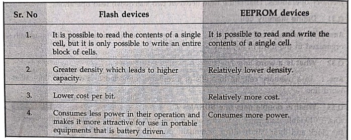
Flash devices
1.
It is possible to read the contents of a single cell, but it is only possible
to write an entire block of cells.
2.Greater
density which leads to higher capacity.
3.Lower
cost per bit.
4.Consumes
less power in their operation and makes it more attractive for use in portable equipments
that is battery driven.
EEPROM devices
1.It
is possible to read and write the contents of a single cell.
2.Relatively
lower density.
3.Relatively
more cost.
4.Consumes
more power.
41. What
is secondary storage ?
Answer: Secondary storage is
non–volatile, high–capacity memory used to store data and programs permanently.
Examples
: HDD, SSD, CDs, DVDs, magnetic tapes.
42. State
any two characteristics of secondary storage.
•
It is non–volatile, meaning data is
retained without power.
•
It has high storage capacity, often
in TB or PB.
43. Why
is secondary storage slower than primary memory?
Answer: Secondary storage
devices (HDDs, SSDs) require physical movement (in HDDs) or internal controller
operations (in SSDs), making access slower than RAM or cache.
44. Why
is secondary storage cost–effective?
Answer: Secondary storage uses
cheaper technologies (Magnetic or flash memory), making the cost per bit much
lower than registers, cache, or RAM.
45. What
is an HDD ?
Answer: A hard disk drive is a
non–volatile magnetic storage device with spinning platters and read /write
heads. It provides large capacity at low cost.
46. What
is an SSD?
Answer: A Solid State Drive
stores data in NAND flash memory without moving parts. It is much faster,
silent and more durable than HDDs.
47. What
is optical storage?
Answer: Storage using laser
technology such as CDs, DVDs, Blu–ray.
Used for media distribution and backups.
48. What
is the function of platters in an HDD?
Answer: Platters are magnetic
disks where data is stored in tracks and
sectors. Multiple platters increase total capacity.
49. What
is the role of the read / write head ?
Answer: The read/write head
detects magnetic patterns while reading and changes magnetic polarity to record
data during writing.
50. What
is the spindle in an HDD ?
Answer: The spindle rotates
the platters at high speeds (5400, 7200, 10,000 RPM) to allow continuous data
access.
51. What
is NAND flash memory ?
Answer: NAND flash is the
primary storage medium in SSDs, storing data as electrical charges inside
memory cells.
52. What
is wear leveling ?
Answer: Wear leveling is a
technique used in SSD controllers to distribute writes evenly across flash
cells, increasing the lifespan of the drive.
53. What
is the role of the SSD controller ?
Answer: The controller manages
read/write operations, wear
leveling, garbage collection, error correction and address mapping.
54. Why
are SSDs faster than HDDs ?
Answer: SSDs have no moving parts, allowing instant
access to data, faster read/write speeds, and low latency.
55. What
is TRIM in SSDs ?
Answer: TRIM is a command that
allows the SSD to erase unused blocks in advance, improving performance and
lifespan.
56. State
two advantages of SSDs.
Answer:
•
Very high read/write speeds
•
More durable and silent (no moving parts).
57. State
two limitations of SSDs.
Answer:
•
Higher cost per gigabyte
•
Limited write cycles due to flash memory wear
58. Which
is more durable : SSD or HDD? Why?
Answer: SSDs are more durable
because they have no mechanical moving
parts, making them resistant to shock and vibration.
59. Which
consumes less power: SSD or HDD ?
Answer: SSDs consume less
power because they operate electronically without motors or spinning disks.
60. What
is cache memory?
Answer:
In
the memory system small section of SRAM is added along with main memory,
referred to as cache memory.
61.
Define hit rate or hit ratio.
Answer: The percentage of
accesses where the processor finds the code or data word it needs in the cache
memory is called the hit rate or hit ratio.
62.
Define miss rate and miss penalty.
Answer: The percentage of
accesses where the processor does not find the code or data word it needs in
the cache memory is called the miss rate. Extra time needed to bring the
desired information into the cache is called the miss penalty.
63.
Define multi–level cache.
Answer: A memory hierarchy
with multiple levels of caches, rather than just a cache and main memory is
called multi–level cache.
64.
Define global miss rate.
Answer: The fraction of
references that miss in all levels of a multilevel cache is called global miss
rate.
65. Define
local miss rate.
Answer: In a multilevel cache
system, the fraction of references to one level of a cache that miss is called
local miss rate.
66. What
is program locality?
Answer: In cache memory
system, prediction of memory location for the next access is essential. This is
possible because computer systems usually access memory from the consecutive
locations. This prediction of next memory address from the current memory
address is known as program locality.
Program locality enables cache controller to get a block of memory instead of
getting just a single address.
67.
Define locality of reference. What are its types ?
Answer: The program may
contain a simple loop, nested loops, or a few procedures that repeatedly call
each other. The point is that many instructions in localized area of the
program are executed repeatedly during some time period and the remainder of
the program is accessed relatively infrequently. This is referred to as locality of reference.
68. Define
the terms : spatial locality and temporal locality.
Answer: Locality of reference
manifests itself in two ways : temporal and spatial. The temporal means that a
recently executed instruction is likely to be executed again very soon. The
spatial means that instructions stored near by to the recently executed
instruction are also likely to be executed soon.
69.
Explain the concept of block fetch.
Answer: Block fetch technique
is used to increase the hit rate of cache. A block fetch can retrieve the data
located before the requested byte (look behind) or data located after the
requested byte (look ahead), or both. When CPU needs to access any byte from
the block, entire block that contains the needed byte is copied from main
memory into cache.
70. Name
the common replacement algorithms.
Answer: The four most common
replacement algorithms are :
1.
Least–Recently Used (LRU)
2.
First–In–First–Out (FIFO)
3.
Least–Frequently–Used (LFU)
4.
Random
71. What
is a mapping function ?
Answer: Usually, the cache
memory can store a reasonable number of blocks at any given time, but this
number is small compared to the total number of blocks in the main memory. The
correspondence between the main memory blocks and those in the cache is
specified by a mapping function.
72. List
the mapping techniques.
Answer: There are two main
mapping techniques which decides the cache organization :
1.
Direct–mapping technique
2.
Associative–mapping technique
The
associative mapping technique is further classified as fully associative and
set associative techniques.
73.
Define direct–mapped cache.
Answer: Direct–mapped cache is
a cache structure in which each memory location is mapped to exactly one
location in the cache.
74.
Define fully associative cache.
Answer: Fully associative
cache is cache structure is which a block can be placed in any location in the
cache.
75.
Define set–associative cache.
Answer: Set–associative cache
is a cache that has a fixed number of locations (at least two) where each block
can be placed.
76.
Define tag field related to memory.
Answer: A field in a table
used for a memory hierarchy that contains the address information required to identify
whether the associated block in the hierarchy corresponds to a requested word
is called tag bit.
77.
Define valid bit related to memory.
Answer: A field in the tables
of a memory hierarchy that indicates that the associated block in the hierarchy
contains valid data is called valid bit.
78. Define
split cache.
Answer: A scheme in which a
level of the memory hierarchy is composed of two independent caches that
operate in parallel with each other, with one handling instructions and one
handling data is called split cache.
79. What
is the need of cache updating?
Answer: In a cache system, two
copies of same data can exist at a time, one in cache and one in main memory.
If one copy is altered and other is not, two different sets of data become
associated with the same address. To prevent this cache updating is needed.
80. Name
the different cache updating systems.
Answer: The different cache
updating systems are :
• Write through system
• Buffered write through system and
• Write–back system
81. What
is a hit ?
Answer: A successful access to
data in cache memory is called hit.
82. Define
cache line or cache block.
Answer: Cache block is used to
refer to a set of contiguous address locations of some size that can be either
present or not present in a cache. Cache block is also referred to as cache
line.
83. What
are the two ways in which the system using cache can proceed for a write
operation?
Answer: Write through protocol
technique.
Write–back
or copy back protocol technique.
84. What
is write through protocol ?
Answer: In write through
updating system, the cache controller copies data to the main memory
immediately after it is written to the cache. Due to this main memory always
contains a valid data, and any block in the cache can be overwritten
immediately without data loss.
85. What
is write–back or copy back protocol ?
Answer: In a write–back
System, the alter bit in the tag field is used to keep information of the new
data. Cache controller checks this bit before overwriting any block in the
cache. If it is set, the controller copies the block to main memory before
loading new data into the cache.
86. When
does a read miss occur?
Answer: When the addressed
word in a read operation is not in the cache, a read miss occur.
87. What
is write miss ?
Answer: During the write
operation if the addressed word is not in cache then said to be write miss.
88. What
is load–through or early restart?
Answer: When a read miss
occurs for a system with cache the required word may be sent to the processor
as soon as it is read from the main memory instead of loading into the cache.
This approach is called load through or early restart and it reduces the
processor's waiting period.
89. What
is replacement algorithm ?
Answer: When the cache is full
and a memory word that is not in the cache is referenced, the cache control
hardware must decide which block should be removed to create space for the new
block that contains the reference word. The collection of rules for making this
decision constitutes the replacement algorithm.
90. What
do you mean by Least Recently Used (LRU)?
Answer: A replacement scheme
in which the block replaced is the one that has been unused for the longest
time is called least recently used replacement scheme.
91. What
are the various memory technologies ?
Answer: Computer memory is
classified as primary memory and secondary memory. Memory technologies in use
for primary memory are : static RAM, Dynamic RAM, ROM and its types (PROM,
EPROM, EEPROM) etc. Memory technologies in use for secondary memory are optical
disk, flash–based removal memory card, hard–disk drives, magnetic tapes etc.
92. What
is NUMA and how is it different from UMA?
Answer: NUMA (Non–Uniform
Memory Access) is a memory architecture in which a processor accesses its own
local memory faster than the memory attached to other processors. In UMA, all
processors share the same memory with equal access time, while in NUMA, local
access is faster and remote access is slower due to interconnect latency.
93. What
is a NUMA Node? Explain local and remote memory access.
Answer:
A
NUMA Node consists of one or more processors (or cores) and the directly
attached local memory.
• Local access :
Processor accesses its own node's memory – fast, low latency.
• Remote access :
Processor accesses memory of another node – slow due to interconnect traversal.
94. Why
was NUMA architecture developed ?
Answer:
NUMA
was developed to overcome the memory bottleneck of UMA systems. As the number
of processors increased, shared memory access caused contention and degraded
performance. NUMA divides memory so that each processor gets high speed access
to its own local memory.
95. What
is NUMA awareness in operating systems ?
Answer:
NUMA–aware
operating systems optimize performance by scheduling processes and allocating
memory within the same NUMA node. They ensure process affinity (keeping a process on one node) and memory
affinity (allocating memory near the processor using it) to reduce remote
memory access.
96. List
any two advantages and any two limitations of NUMA.
Answer:
Advantages :
1.
High memory bandwidth.
2.
Better scalability for multiprocessor systems.
Limitations :
1.
Remote memory access is slower.
2.
Software requires optimization for memory locality.
97.
Explain how cache coherence is maintained in NUMA systems.
Answer: NUMA systems use
memory controllers and protocols like directory–based
coherence or snooping to ensure
all processors see consistent data. These mechanisms update or invalidate cache
entries across nodes when shared data changes.
98. What
is the need for error detection and correction in memory systems ?
Answer: Electrical
interference, noise, or hardware faults can cause bits to flip during the
storage or transmission of data. This leads to corrupted data. Therefore,
memory systems use error detection and error correction codes (EDC/ECC) to
ensure data reliability. They detect when a bit is corrupted and, in many
cases, can correct it automatically.
99. What
is a parity bit ? How does it help in detecting errors ?
Answer: A parity bit is an
extra bit added to every data word to make the total number of 1s either even (even parity) or odd (odd parity). When
data is read back, parity is recalculated.
•
If parity matches → No error
•
If parity mismatches → Error detected
However,
parity can only detect single–bit
errors; it cannot correct them.
100.
Explain the basic principle of Hamming code.
Answer:
Hamming
code adds several parity bits at positions that are powers of 2 (1, 2, 4,
8...). Each parity bit covers a specific group of data bits. When a word is
read, new parity checks generate a syndrome.
•
Syndrome = 0000 → No error
•
Syndrome # 0000 → Binary value of syndrome gives the bit position in error.
The
bit is corrected by flipping it. Thus, Hamming code provides single–bit error correction.
101. What
is a syndrome in Hamming code? How is it used ?
Answer:
A
syndrome is a 4–bit or 3–bit binary pattern generated from the check bits (C8,
C4, C2, C1).
It
indicates the position of the erroneous bit :
•
If syndrome = 000 → No error
•
If syndrome = Binary number k → Error in bit k
Thus,
syndrome directly helps in identifying and correcting single–bit errors.
102.
Write the formula relating the number of data bits (n) and parity bits (k) in
Sylle Hamming code.
Answer: The Hamming code must
satisfy :
2k
– 1 ≥ n + k
This
ensures that there are enough parity bits to uniquely identify all bit
positions (Data + Parity).
Example :
For n = 8 data bits, k = 4 parity bits are required.
103. What
is SECDED? Explain its usefulness.
Answer: SECDED stands for single error correction and double error
detection. It is an extension of Hamming code created by adding an extra
parity bit (P13). This additional bit allows :
•
Correction of single–bit errors
•
Detection of double–bit errors (though
not correctable). This improves fault tolerance in memory systems like RAM.
104. List
the four possible cases when using SECDED.
Answer:
Using
Hamming syndrome (C8C4C2C1) and overall parity (P13) :
1. C = 0, P = 0
→ No error
2. C ≠ 0, P = 1 → Single–bit
error → Correctable
3. C ≠ 0, P = 0
→ Double–bit error → Detected, not correctable
4. C = 0, P = 1
→ Error in overall parity bit (P13)
Digital Principles and Computer Organization: Chapter 11: Memory : Tag: : Digital Principles and Computer Organization - Memory: Two Marks Important Questions and Answers
Digital Principles and Computer Organization: Chapter 11: Memory
Under Subject

Digital Principles and Computer Organization
CS25C06 2nd Semester AIDS, CSE, IT, CSE(CY) Dept | 2025 Regulation | 2nd Semester 2025 Regulation
Related Subjects

English Essentials II
EN25C02 2nd Semester | 2025 Regulation | 2nd Semester 2025 Regulation

Tamils and Technology தமிழர்களும் தொழில்நுட்பமும்
UC25H02 2nd Semester | 2025 Regulation | 2nd Semester 2025 Regulation

Linear Algebra
MA25C02 2nd Semester | 2025 Regulation

Applied Physics (CSIE) II
PH25C03 2nd Semester AIDS, CSE, IT, CSE(CY) Dept | 2025 Regulation | 2nd Semester 2025 Regulation
Digital Principles and Computer Organization
CS25C06 2nd Semester AIDS, CSE, IT, CSE(CY) Dept | 2025 Regulation | 2nd Semester 2025 Regulation

Basic Electrical and Electronics Engineering
EE25C01 2nd Semester | 2025 Regulation | 2nd Semester 2025 Regulation

Python for Data Science
AD25201 2nd Semester AIDS Dept | 2025 Regulation | 2nd Semester 2025 Regulation

Re-Engineering for Innovation
ME25C05 2nd Semester | 2025 Regulation | 2nd Semester 2025 Regulation

Python for Data Science - Laboratory
AD25201 2nd Semester AIDS Dept | 2025 Regulation | 2nd Semester 2025 Regulation