Digital Principles and Computer Organization: Chapter 11: Memory
Main Memory: RAM, DRAM, ROM, EEPROM
1. RAM (Random Access Memories): Static RAM Cell, CMOS Cell, 2. DRAM (Dynamic RAMs), 3. Comparison between SRAM and DRAM , 4. ROM (Read Only Memories): PROM (Programmable Read Only Memory)., EPROM (Erasable Programmable Read Only Memory), EEPROM (Electrically Erasable Programmable Read Only Memory). Questions: 1. What are the types of RAMs? Explain them in detail. 2. Describe the organization of a typical RAM chip. 3. Write notes on static memories. 4. Describe the working principle of RAM. 5. Draw a CMOS memory cell and explain its function. 6. Differentiate DRAM and SRAM. 7. Write note on ROM technologies. 8. Give the features of a ROM cell. 9. Explain various types of ROMs.
Main Memory
1. RAM (Random Access Memories)
•
Memories that consists of circuits capable of retaining their state as long as
power is applied are known as static memories.
•
These are Random Access Memory (RAM) and hence combinely called static RAM memories.
1. Static RAM Cell
•
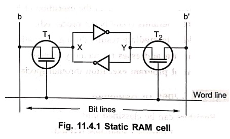
Fig. 11.4.1 shows the implementation of static RAM cell. It consists of two cross–coupled
inverters as a latch and two transistors T1 and T2 which
act as a switches.
•
The latch is connected to two bit lines by transistors T1 and T2.
The word line controls the opening and closing of transistors T1 and
T2. When word line is at logic 0 level (Ground level), the transistors
are off and the latch retains its state.
Read operation
•
For read operation, word line is made logic 1 (high) so that both transistors
are ON. Now if the cell is in state 1, the signal on bit line b is high and the
signal on bit line b' is low. The opposite is true if the cell is in state 0.
The b and b' are complements of each other. The sense/write circuits connected
to the bit lines monitor the states of b and b' and set the output accordingly.
Write operation
•
For write operation, the state to be set is placed on the line b and its
complement is placed on line b' and then the word line is activated. This
action forces the cell into the corresponding state and write operation is
completed.
2. CMOS Cell
•
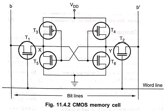
Fig. 11.4.2 shows the CMOS cell. Here, transistor pairs (T3, T5)
and (T4, T6) form the cross–coupled inverters and transistors T1
and T2 act as a switches. The latch is connected to two bit lines by
transistors T1 and T2.
•
The word line controls the opening and closing of transistors T1 and
T2. When word line is at logic 0 level (Ground level), the
transistors T1 and T2 are off and the latch retains its
state.
Read operation
•
For read operation, word line is made high to switch–on transistor T1
and T2. The cell is in state 1, if voltage at point X is maintained
high by having transistors T3 and T6 on, while T4 and
T5 are off. The cell is in state 0, if the voltage at point X is
maintained low by having transistors T3 and T6 off, while
T4 and T5 are on.
Write operation
•
For write operation, the state to be set is placed on the line b and its
complement is placed on line b', and then the word line is activated. This
action forces the cell into the corresponding state.
2. DRAM (Dynamic RAMs)
•
Dynamic RAM stores the data as a charge on the capacitor. Fig. 11.4.3 shows the
dynamic RAM cell.
•
A dynamic RAM contains thousands of such memory cells.
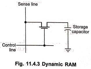
• When COLUMN (Sense) and ROW (Control) lines go high, the MOSFET conducts and charges the capacitor.
•
When the COLUMN and ROW lines go low, the MOSFET opens and the capacitor retains
its charge. In this way, it stores 1 bit.
•
Since only a single MOSFET and capacitor are needed, the dynamic RAM contains
more memory cells as compared to static RAM per unit area.
•
The disadvantage of dynamic RAM is
that it needs refreshing of charge on the capacitor after every few
milliseconds. This complicates the system design, since it requires the extra
hardware to control refreshing of dynamic RAMs.
3. Comparison between SRAM and DRAM
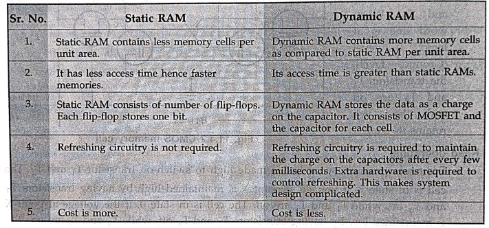
Static RAM
1.
Static RAM contains less memory cells per unit area.
2.
It has less access time hence faster memories.
3.
Static RAM consists of number of flip–flops. Each flip–flop stores one bit.
4.
Refreshing circuitry is not required.
5.
Cost is more.
Dynamic RAM
1.
Dynamic RAM contains more memory cells as compared to static RAM per unit area.
2.
Its access time is greater than static RAMs.
3.
Dynamic RAM stores the data as a charge on the capacitor. It consists of MOSFET
and the capacitor for each cell.
4.
Refreshing circuitry is required to maintain the charge on the capacitors after
every few milliseconds. Extra hardware is required to control refreshing. This
makes system design complicated.
5.
Cost is less.
4. ROM (Read Only Memories)
•
We can't write data in Read Only Memories (ROM). It is non–volatile memory i.e.
it can hold data even if power is turned off.
•
Generally, ROM is used to store the binary codes for the sequence of
instructions and data such as look up Read tables. This is because this type of
information does not change.
•
ROMs are also accessed randomly with unique addresses.
•
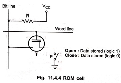
Fig. 11.4.4 shows the typical configuration of a ROM cell. It consists of a
transistor T and switch P.
•
The transistor T is driven by the word line.
•
The contents of cell can be read from the cell when word line is logic 1.
•
A logic value 0 is read if the transistor is connected to ground through switch
P. If switch P is open, a logic value 1 is read.
•
The bit line is connected through a resistor to the power supply.
•
A sense circuit at the end of the bit line generates the proper output value.
•
Data is stored into a ROM when it is manufactured.
•
There are four types of ROM : Masked ROM, PROM, EPROM and EEPROM or E2PROM.
1. PROM (Programmable Read Only Memory)
•
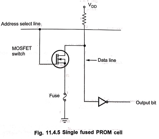
PROMs are programmed by user. To provide the programming facility, each address
select and data line intersection has its own fused MOSFET or transistor.
•
When the fuse is intact, the memory cell is configured as a logic 1 and when
fuse is blown (open circuit), the memory cell is logical 0.
•
Logical 0s are programmed by selecting the appropriate select line and then
driving the vertical data line with a pulse of high current.
•
Fig. 11.4.5 shows a PROM fused MOSFET memory cell
•
The fuse uses material like nichrome and polycrystalline. For blowing the fuse
it is necessary to pass around 20 to 50 mA of current for period 5 to 20 μs. The
blowing of fuses according to the truth table called programming of ROM.
•
The PROMs are one time programmable. Once programmed, the information stored is
permanent.
2. EPROM (Erasable Programmable Read Only Memory)
•
Erasable programmable ROMs use MOS circuitry. They store 1's and 0's as a packet
of charge in a buried layer of the IC
chip.
•
EPROMS can be programmed by the user with a special EPROM programmer.
•
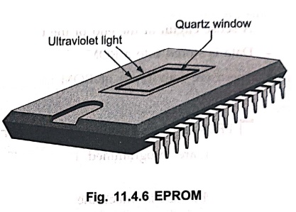
The important point is that we can erase the stored data in the EPROMs by
exposing the chip to ultraviolet light through its quartz window for 15 to 12 minutes,
as shown in Fig. 11.4.6.
•
It is not possible to erase selective information, when erased the entire
information is lost.
•
The chip can be reprogrammed.
•
This memory is ideally suitable for product development, experimental projects and
college laboratories, since this chip can be reused many times.
EPROM Programming :
•
When erased each cell in contains 1. Data is introduced by selectively
programming 0's into the desired bit locations. Although only 0's will be
programmed, both 1's and 0's can be presented in the data.
•
During programming address and data are applied to address and data pins of the
EPROM. When the address and data are stable, program pulse is applied to the
program input of the EPROM. The program pulse duration is around 50 ms and its
amplitude depends on EPROM IC. It is
typically 5.5 V to 25 V.
•
In EPROM, it is possible to program any location at any time – either individually,
sequentially or at random.
3. EEPROM (Electrically Erasable Programmable Read Only Memory)
•
Electrically erasable programmable ROMs also use MOS circuitry very similar to
that of EPROM.
•
Data is stored as charge or no charge on an insulated layer or an insulated
floating gate in the device.
•
The insulating layer is made very thin (< 200
•
EEPROM allows selective erasing at the register level rather than erasing all
the information since the information can be changed by using electrical
signals.
•
The EEPROM memory also has a special chip erase mode by which entire chip can
be erased in 10 ms. This time is quite small as compared to time required to
erase EPROM. It can be erased and reprogrammed with device right in the
circuit.
Disadvantage
•
EEPROMS are most expensive and the least dense ROMs.
Review Questions
1. What are the types
of RAMs? Explain them in detail.
2. Describe the
organization of a typical RAM chip.
3. Write notes on
static memories.
4. Describe the
working principle of RAM.
5. Draw a CMOS memory cell
and explain its function.
6. Differentiate DRAM
and SRAM.
7. Write note on ROM
technologies.
8. Give the features
of a ROM cell.
9. Explain various
types of ROMs.
Digital Principles and Computer Organization: Chapter 11: Memory : Tag: : - Main Memory: RAM, DRAM, ROM, EEPROM
Digital Principles and Computer Organization: Chapter 11: Memory
Under Subject

Digital Principles and Computer Organization
CS25C06 2nd Semester AIDS, CSE, IT, CSE(CY) Dept | 2025 Regulation | 2nd Semester 2025 Regulation
Related Subjects

English Essentials II
EN25C02 2nd Semester | 2025 Regulation | 2nd Semester 2025 Regulation

Tamils and Technology தமிழர்களும் தொழில்நுட்பமும்
UC25H02 2nd Semester | 2025 Regulation | 2nd Semester 2025 Regulation

Linear Algebra
MA25C02 2nd Semester | 2025 Regulation

Applied Physics (CSIE) II
PH25C03 2nd Semester AIDS, CSE, IT, CSE(CY) Dept | 2025 Regulation | 2nd Semester 2025 Regulation
Digital Principles and Computer Organization
CS25C06 2nd Semester AIDS, CSE, IT, CSE(CY) Dept | 2025 Regulation | 2nd Semester 2025 Regulation

Basic Electrical and Electronics Engineering
EE25C01 2nd Semester | 2025 Regulation | 2nd Semester 2025 Regulation

Python for Data Science
AD25201 2nd Semester AIDS Dept | 2025 Regulation | 2nd Semester 2025 Regulation

Re-Engineering for Innovation
ME25C05 2nd Semester | 2025 Regulation | 2nd Semester 2025 Regulation

Python for Data Science - Laboratory
AD25201 2nd Semester AIDS Dept | 2025 Regulation | 2nd Semester 2025 Regulation