Digital Principles and Computer Organization: Chapter 7: Sequential Circuits - Registers
Ring Counters
Sequential Circuits
Questions: 1. Draw a six stage ring counter and explain its operation. 2. Draw the timing diagram of 4-bit ring counter. 3. Draw a 2-bit ripple counter and convert this into a 2-bit ring counter. 4. Explain the operation of shift and ring counters. 5. Design a 3 bit ring counter and find the mod of the designed counter.
Ring Counters
•
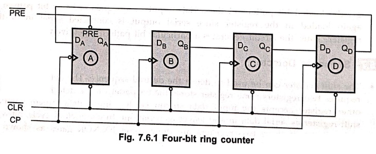
Fig. 7.6.1 shows the logic diagram for four–bit ring counter. As shown in the
bale Fig. 7.6.1, the Q output of each stage is connected to the D input of the
next stage and the output of last stage is fed back to the input of first
stage. The  followed by
  makes the output
of first stage to '1' and remaining outputs are zero, i.e. QA is one
and QB, QC,QD are zero.
makes the output
of first stage to '1' and remaining outputs are zero, i.e. QA is one
and QB, QC,QD are zero.
•
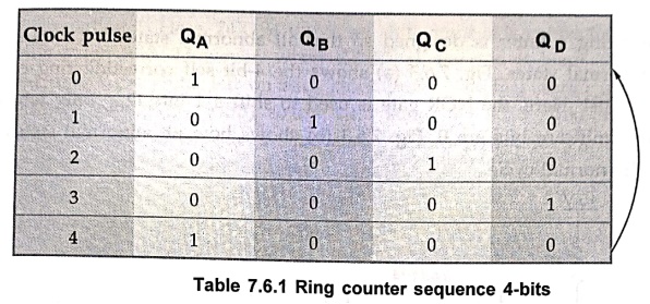
The first clock pulse produces QB = 1 and remaining outputs are
zero. According to the clock pulses applied at the clock input CP, a sequence
of four states is produced. These states are listed in Table 7.6.1.
•
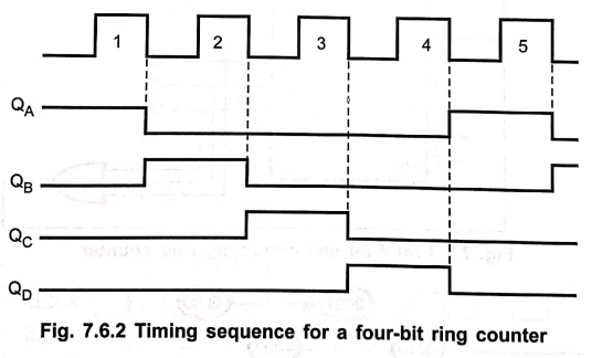
As shown in Table 7.6.1, 1 is always retained in the counter and simply shifted
'around the ring', advancing one stage for each clock pulse. In this case four
stages of flip–flops are used. So a sequence of four states is produced and
repeated. Fig. 7.6.2 gives the timing sequence for a four–bit ring counter.
•
The ring counter can be used for counting the number of pulses. The number of
pulses counted is read by noting which flip–flop is in state 1. No decoding
circuitry is required. Since there is one pulse at the output for each of the N
clock pulses, this circuit is also referred to as a divide–by–N–counter or an N
: 1 scalar. Ring counters can be instructed for any desired MOD number, that is
MOD–N ring counter requires N flip–flops.
Self correcting counters
•
The ring counters suffer from one major problem–if its single 1 output is lost
due to a temporary hardware problem (e.g. noise), the counter goes to state
0000 and stays there forever. Likewise, if an extra 1 output is set (i.e. state
0101 is created), the counter will go through an incorrect cycle of states and
may stay in that cycle forever.
•
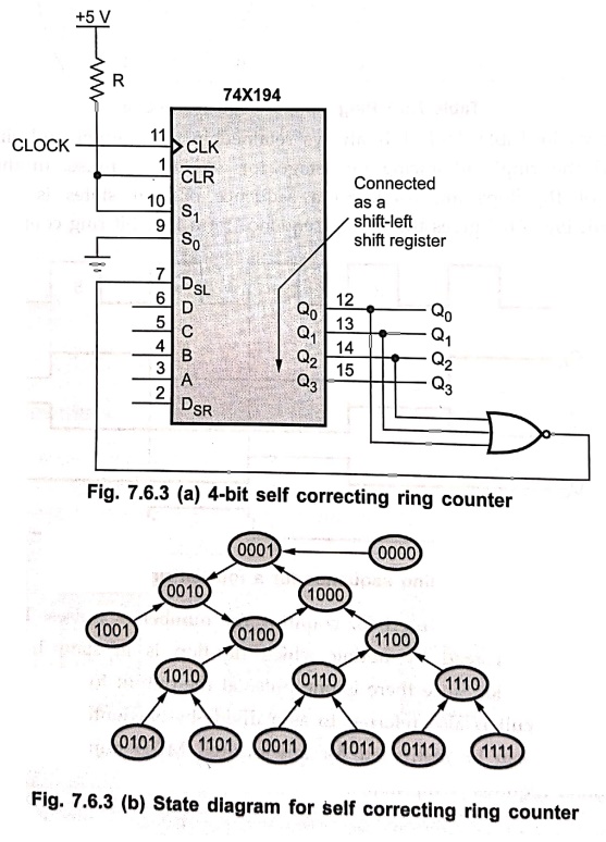
A self correcting counter is designed so that all abnormal states have
transitions leading to normal states. Fig. 7.6.3 (a) shows the 4–bit self correcting
ring counter using IC 74X194. Here, the NOR gate is used to shift a 1 into DSL
only when the three least significant bits are 0. Fig. 7.6.3 (b) shows how all
abnormal states lead back into the normal cycle.
•
The ring counter shown above has a single circulating 1. The ring counter with
a single circulating 0 can be designed using NAND gate instead of NOR gate in
Fig. 7.6.3 (a).
Example: 1
Design a 4–bit, 4–state
ring counter using 74X194.
Solution :
Fig.
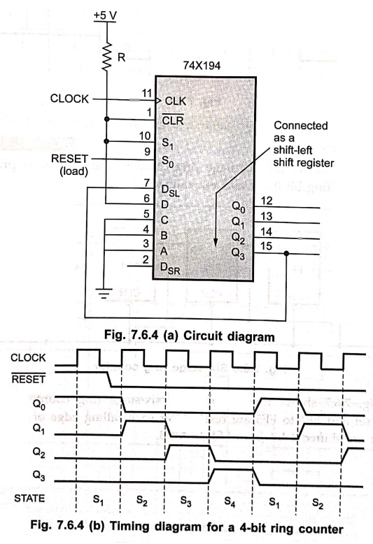
7.6.4 (a) shows the circuit diagram for a 4–bit, 4–state ring counter with a
single circulating 1. Here, 74X194 universal shift register is connected so
that it normally performs a left–shift. However, when RESET is asserted it
loads 0001. Once RESET is negated, the 74194 shifts left on each clock pulse.
The DSL serial input is connected to the leftmost output (Q3 : MSB)
so the next states are 0010, 0100, 1000, 0001, 0010, .... Thus the counter
visits four unique states before repeating. Fig. 7.6.4 (b) shows the timing
diagram for this 4–bit counter.
Example: 2
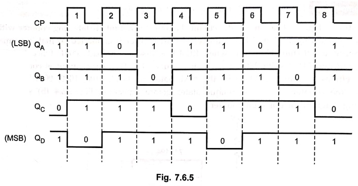
Assume that 1011 input
data pattern is loaded into a 4–bit ring counter. Sketch the resulting flip–flop
Q output waveforms (Assume positive edge triggering).
Solution :
Example: 3
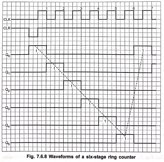
Draw a six stage ring
counter and explain its operation. Mention about the use of presetting the
counter.
Solution :
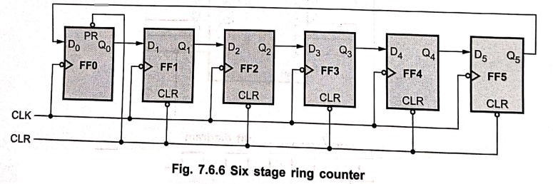
Fig.
7.6.6 shows the six stage ring counter. The counter is present to value
(000001)2 by setting bit 0 = 1 and remaining bits = 0.
Operation :
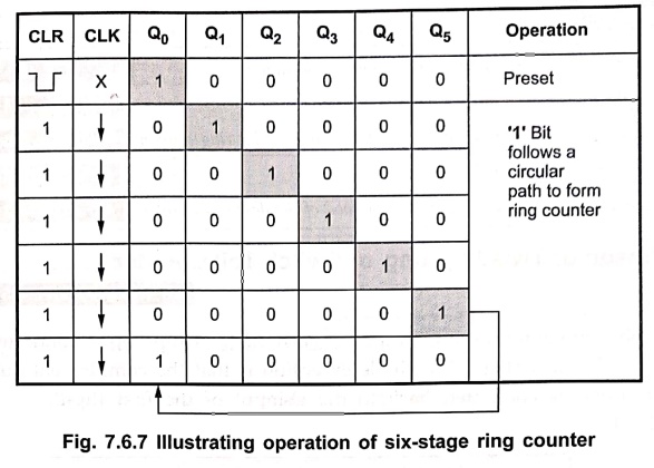
Fig. 7.6.7 shows the operation of six–stage ring counter. On preset, FF0 (flip–flop
0) is set and FF1 to FF5 are reset. After each falling edge of the clock
contents of ring counter are shifted 1 bit from LSB to MSB.
Waveform :
Review Questions
1. Draw a six stage
ring counter and explain its operation.
2. Draw the timing
diagram of 4–bit ring counter.
3. Draw a 2–bit ripple
counter and convert this into a 2–bit ring counter.
4. Explain the operation
of shift and ring counters.
5. Design a 3 bit ring
counter and find the mod of the designed counter.
Digital Principles and Computer Organization: Chapter 7: Sequential Circuits - Registers : Tag: : Sequential Circuits - Ring Counters
Digital Principles and Computer Organization: Chapter 7: Sequential Circuits - Registers
Under Subject

Digital Principles and Computer Organization
CS25C06 2nd Semester AIDS, CSE, IT, CSE(CY) Dept | 2025 Regulation | 2nd Semester 2025 Regulation
Related Subjects

English Essentials II
EN25C02 2nd Semester | 2025 Regulation | 2nd Semester 2025 Regulation

Tamils and Technology தமிழர்களும் தொழில்நுட்பமும்
UC25H02 2nd Semester | 2025 Regulation | 2nd Semester 2025 Regulation

Linear Algebra
MA25C02 2nd Semester | 2025 Regulation

Applied Physics (CSIE) II
PH25C03 2nd Semester AIDS, CSE, IT, CSE(CY) Dept | 2025 Regulation | 2nd Semester 2025 Regulation
Digital Principles and Computer Organization
CS25C06 2nd Semester AIDS, CSE, IT, CSE(CY) Dept | 2025 Regulation | 2nd Semester 2025 Regulation

Basic Electrical and Electronics Engineering
EE25C01 2nd Semester | 2025 Regulation | 2nd Semester 2025 Regulation

Python for Data Science
AD25201 2nd Semester AIDS Dept | 2025 Regulation | 2nd Semester 2025 Regulation

Re-Engineering for Innovation
ME25C05 2nd Semester | 2025 Regulation | 2nd Semester 2025 Regulation

Python for Data Science - Laboratory
AD25201 2nd Semester AIDS Dept | 2025 Regulation | 2nd Semester 2025 Regulation