Digital Principles and Computer Organization: Chapter 7: Sequential Circuits - Registers
Applications of Shift Registers
1. Delay Line 2. Serial-to-Parallel Converter 3. Parallel-to-Serial Converter 4. Shift Register Counters 5. Pseudo-Random Binary Sequence (PRBS) Generator 6. Sequence Generator 7. Sequence Detector
Applications of Shift
Registers
• We have seen that primary use of shift register is temporary data storage and bit manipulations. Some of the common applications of shift registers are as discussed below.
1. Delay Line
•
A Serial–In–Serial–Out (SISO) shift register can be used to introduce time
delay ∆t in digital signals. The time delay can be given as
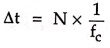
∆t = N × 1/fc
where
N is the number of stages (i.e. flip–flops) and fc is the clock
frequency.
•
Thus, an input pulse train appears at the output delayed by ∆t. The amount of
delay can be controlled by the clock frequency or by the number of flip–flops
in the shift register.
2. Serial–to–Parallel Converter
•
A Serial–In–Parallel–Out (SIPO) shift register can be used to convert data in
the serial form to the parallel form.
3. Parallel–to–Serial Converter
•
A Parallel–In–Serial–Out (PISO) shift register can be used to convert data in
the parallel form to the serial form.
4. Shift Register Counters
•
A shift register can also be used as a counter. A shift register with the
serial output connected back to the serial input is called shift register counter.
Because of such a connection, special specified sequences are produced as the
output. The most common shift register counters are the ring counter and the
Johnson counter.
5. Pseudo–Random Binary Sequence (PRBS) Generator
•
Another important application of shift register is a pseudo–random binary
sequence generator. Here, suitable feedback is used to generate pseudo–random
sequence. The term random here means that the outputs do not cycle through a
normal binary count sequence. The term pseudo here refers to the fact that the
sequence is not truly random because it does cycle through all possible
combinations once every 2n – 1 clock cycles, where n represents the
number of shift register stages (number of flip–flops).
6. Sequence Generator
•
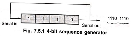
The shift register can be used to generate a particular bit pattern
repetitively. Fig. 7.5.1 shows the basic block diagram of a sequence generator.
Here, left most flip–flop input accept input accept the Serial in serial input
and the right most flip–flop gives serial data output. It is important to note
that the serial data output signal is connected as a serial data in. On every
clock pulse the data shift operation takes place. We get the loaded bit pattern
at the serial output in a sequence. Same bit pattern is again loaded in the
register since serial output is connected serial in of the register. Thus, the
circuit generates a particular bit pattern repetitively.
7. Sequence Detector
•
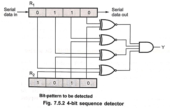
The shift register can be used to detect the desired sequence. The detection
process requires two registers : one register stores the bit pattern to be
detected i.e. R1 and other register accepts the input data stream
i.e. R2. Input data stream enters a shift register as serial data in
and leaves as serial out. In every clock cycle, bit–wise comparisons of these
two registers are done using EX–NOR gates as shown in Fig. 7.5.2. We know that,
the two–input EX–NOR gate gives logic high output when both inputs are either
low or high, i.e. when both are equal. When outputs of all the EX–NORS gates
are logic high we can say that all bits are matched and hence the desired bit
pattern is detected. The final output which indicates that the pattern is
detected is taken from four–input AND gate.
•
The 4–bit sequence detector shown in Fig. 7.5.2 can be made programmable by
loading the desired 4–bit data in the register R2.
Review Question
1. Explain the
applications of shift registers.
Digital Principles and Computer Organization: Chapter 7: Sequential Circuits - Registers : Tag: : - Applications of Shift Registers
Digital Principles and Computer Organization: Chapter 7: Sequential Circuits - Registers
Under Subject

Digital Principles and Computer Organization
CS25C06 2nd Semester AIDS, CSE, IT, CSE(CY) Dept | 2025 Regulation | 2nd Semester 2025 Regulation
Related Subjects

English Essentials II
EN25C02 2nd Semester | 2025 Regulation | 2nd Semester 2025 Regulation

Tamils and Technology தமிழர்களும் தொழில்நுட்பமும்
UC25H02 2nd Semester | 2025 Regulation | 2nd Semester 2025 Regulation

Linear Algebra
MA25C02 2nd Semester | 2025 Regulation

Applied Physics (CSIE) II
PH25C03 2nd Semester AIDS, CSE, IT, CSE(CY) Dept | 2025 Regulation | 2nd Semester 2025 Regulation
Digital Principles and Computer Organization
CS25C06 2nd Semester AIDS, CSE, IT, CSE(CY) Dept | 2025 Regulation | 2nd Semester 2025 Regulation

Basic Electrical and Electronics Engineering
EE25C01 2nd Semester | 2025 Regulation | 2nd Semester 2025 Regulation

Python for Data Science
AD25201 2nd Semester AIDS Dept | 2025 Regulation | 2nd Semester 2025 Regulation

Re-Engineering for Innovation
ME25C05 2nd Semester | 2025 Regulation | 2nd Semester 2025 Regulation

Python for Data Science - Laboratory
AD25201 2nd Semester AIDS Dept | 2025 Regulation | 2nd Semester 2025 Regulation