Digital Principles and Computer Organization: Chapter 7: Sequential Circuits - Registers
Types of Shift Registers
1. Serial In Serial Out (SISO) Shift Register 2. Serial In Parallel Out (SIPO) Shift Register 3. Parallel In Serial Out (PISO) Shift Register 4. Parallel In Parallel Out (PIPO) Shift Register 5. Bidirectional Shift Register
Types of Shift
Registers
1. Serial
In Serial Out (SISO) Shift Register
Shift
left mode
•
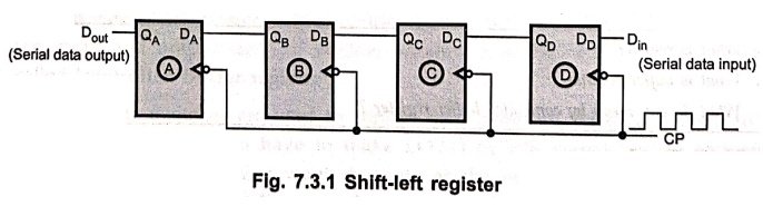
Fig. 7.3.1 shows serial–in serial–out shift–left register.
•
We will illustrate the entry of the four bit binary number 1111 into the
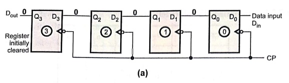
register, beginning with the left–most bit. Initially, register is cleared. So
QAQBQCQ0 = 0 0 0 0
a)
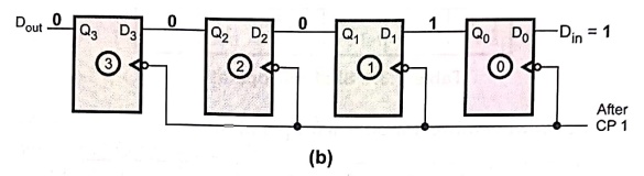
When data 1 1 1 1 is applied serially, i.e. left–most 1 is applied as Din,
Din = 1 , Q3 Q2 Q1Q0 = 0
0 0 0. The arrival of the first falling clock edge sets the right–most flip–flop,
and the stored word becomes, Q3Q2Q1Q0 = 0 0 0 1
b)
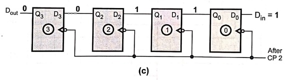
When the next negative clock edge hits, the Q1 flip–flop sets and
the register contents become, Q3Q2Q1Q0
= 0 0 1 1
c)
The third negative clock edge results in, Q3Q2Q1Q0
= 0 1 1 1
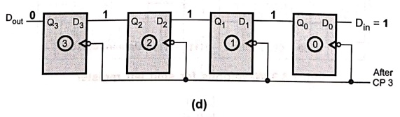
d)
The fourth falling clock edge gives, Q3Q2Q1Q0
= 1 1 1 1.
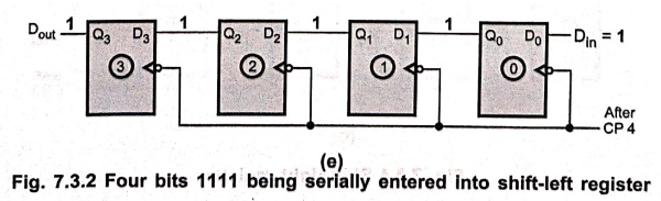
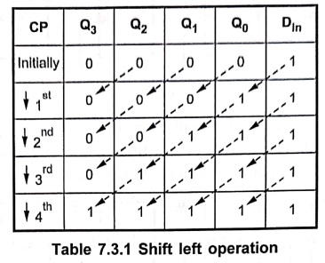
•
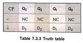
Table 7.3.1 summarizes the shift left operation.
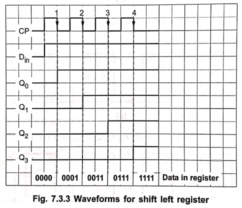
•
Fig. 7.3.3 shows waveforms for shift left operation
Shift
right mode
•
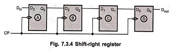
Fig. 7.3.4 shows serial–in serial–out shift–right register.
•
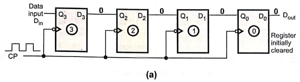
We will illustrate the entry of the four bit binary number 1111 into the
register, beginning with the left–most bit.
•
Initially, register is cleared. So Q3Q2Q1Q0
= 0 0 0 0
a)
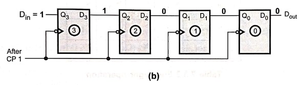
When data 1 1 1 1 is applied serially, i.e. left–most 1 is applied as Din,
Din
= 1, Q3 Q2 Q1Q0 = 0 0 0 0
The
arrival of the first falling clock edge sets the left–most flip–flop and the
stored word becomes, Q3Q2Q1Q0 = 1 0
0 0
b)
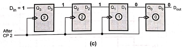
When the next falling clock edge hits, the Q2 flip–flop sets and the
register contents become, Q3Q2Q1Q0
= 1100
c)
The third falling clock edge results in, Q3Q2Q1Q0
= 1110.
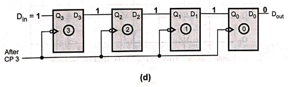
d)
The fourth falling clock edge gives, Q3Q2Q1Q0
= 1111.
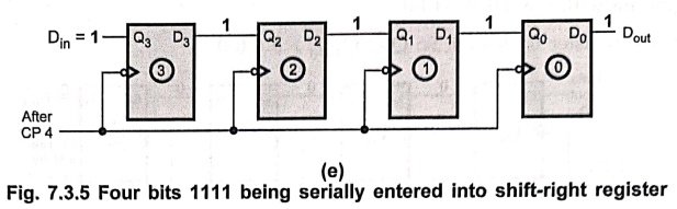
•
Table 7.3.2 summarizes the shift right operation.
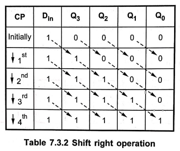
•
Fig. 7.3.6 shows waveforms for shift right operation.
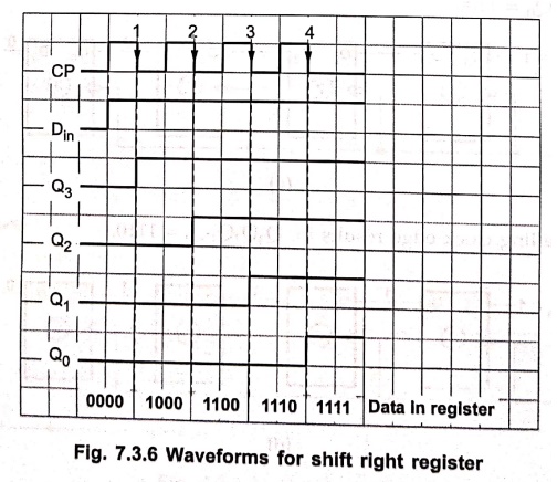
2. Serial
In Parallel Out (SIPO) Shift Register
•
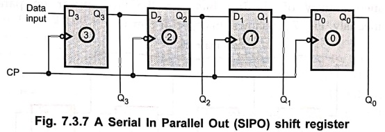
In this case, the data bits are entered into the register in the same manner as
discussed in the last section, i.e. serially. But the output is taken in
parallel. Once the data are stored, each bit appears on its respective output
line and all bits are available pants simultaneously, instead of on a bit–by–bit
basis as with the serial output as shown in Fig. 7.3.7.
3.
Parallel In Serial Out (PISO) Shift Register
•
In this type, the bits are entered in parallel i.e simultaneously into their
respective stages on parallel lines.
•
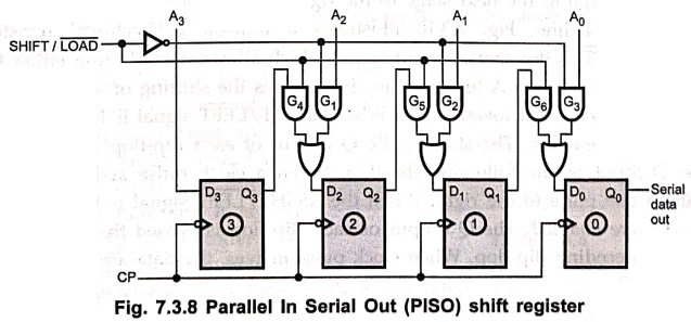
Fig. 7.3.8 illustrates a four–bit parallel in serial out register. There are
four input lines A3, A2, A1, A0 for
entering data in parallel into the register.  is the control input which allows
shift or loading data operation of the register. When is low, gates G1, G2, G3 are enabled, allowing
each input data bit to be applied to D input of its respective flip–flop. When
a clock pulse is applied, the flip–flops with D = 1 will SET and those with D =
0 will RESET. Thus all four bits are stored simultaneously.
is the control input which allows
shift or loading data operation of the register. When is low, gates G1, G2, G3 are enabled, allowing
each input data bit to be applied to D input of its respective flip–flop. When
a clock pulse is applied, the flip–flops with D = 1 will SET and those with D =
0 will RESET. Thus all four bits are stored simultaneously.
•
When is high, gates G1, G2, G3
are disabled and gates G4, G5, G6 are enabled.
This allows the data bits to shift right from one stage to the next. The OR
gates at the D–inputs of the flip–flops allow either the parallel data entry
operation or shift operation, depending on which AND gates are enabled by the
level on the input.
4.
Parallel In Parallel Out (PIPO) Shift Register
•
From the third and second types of registers, it is cleared that how to enter
the data in parallel i.e. all bits simultaneously into the register and how to
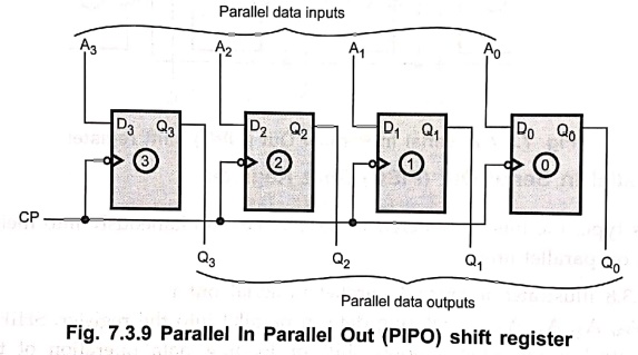
take data out in parallel from the register. In 'parallel in parallel out
register', there is simultaneous entry of all data bits and the bits appear on
parallel outputs simultaneously. Fig. 7.3.9 shows this type of register.
5.
Bidirectional Shift Register
•
This type of register allows shifting of data either to the left or to the
right side. It can be implemented by using logic gate circuitry that enables the
transfer of data from one stage to the next stage to the right or to the left,
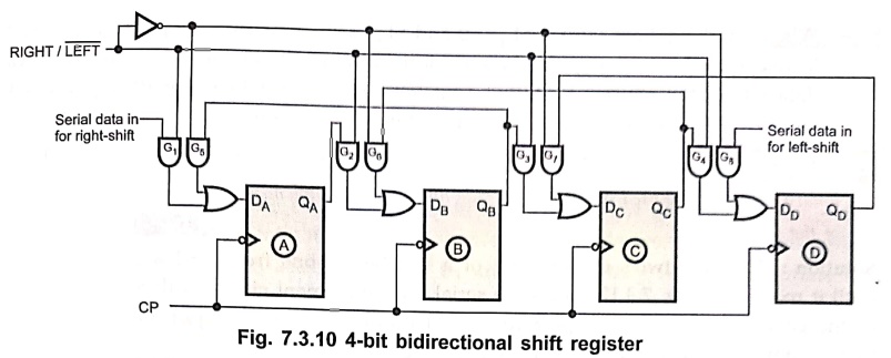
depending on the level of a control line. Fig. 7.3.10 illustrates a four–bit
bidirectional register. The  is the control input
signal which allows data shifting either towards right or towards left. A high
on this line enables the shifting of data towards right and a low enables it
towards left. When signal is high, gates G1, G2,
G3, G4 are enabled. The state of the Q output of each flip–flop
is passed through the D input of the following flip–flop. When a clock pulse
arrives, the data are shifted one place to the right. When the signal is low, gates G5, G6, G7, G8
are enabled. The Q output of each flip–flop is passed through the D input of
the preceding flip–flop. When clock pulse arrives, the data are shifted one
place to the left.
is the control input
signal which allows data shifting either towards right or towards left. A high
on this line enables the shifting of data towards right and a low enables it
towards left. When signal is high, gates G1, G2,
G3, G4 are enabled. The state of the Q output of each flip–flop
is passed through the D input of the following flip–flop. When a clock pulse
arrives, the data are shifted one place to the right. When the signal is low, gates G5, G6, G7, G8
are enabled. The Q output of each flip–flop is passed through the D input of
the preceding flip–flop. When clock pulse arrives, the data are shifted one
place to the left.
Bidirectional
Shift Register with Parallel Load
•
We have seen that shift register can be used for converting serial data into
parallel data, and vice versa. When parallel load capability is added to the
shift register, the data entered in parallel can be taken out in serial fashion
by shifting the data stored in the register. Such a register is called bidirectional
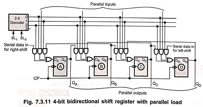
shift register with parallel load. Fig. 7.3.11 shows bidirectional shift
register with parallel load.
•
As shown in Fig. 7.3.11, the D input of each flip–flop has three sources :
Output of left adjacent flip–flop, output of right adjacent flip–flop and
parallel input. Out of these three sources one source is selected at a time and
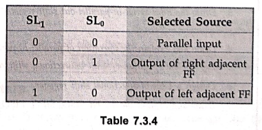
it is done with the help of decoder. The decoder select lines (SL1
and SL0) select the one source out of three as shown in Table 7.3.4.
•
When select lines are 00 (i.e. SL1 = 0 and SL0 = 0), data from the
parallel inputs is loaded into the 4–bit register. When select lines are 01
(i.e. SL1 = 0 and SL0 = 1), data within the register is
shifted 1–bit left. When select lines are 10 (i.e. SL1 = 1 and SL0
= 0), data within the register is shifted 1–bit right.
Example: 1
Design a serial 2's
complement circuit with a shift register and a flipflop. The binary number is
shifted out from one side and its 2's complement a shifted into other side of
the shift register.
Solution :
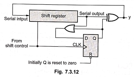
To
get a two's complement of a number of bits from LSB are kept as it is until it
receives 1. Fig. 7.3.12 shows the serial 2's complement circuit with a shift
register. In the circuit, initially Q is kept zero so that output is same as
input. Q is set on the first 1 from × and then each bit is complemented.
Note :
1)
y = x if Q = 0 and y =  if Q
= 1
if Q
= 1
2)
x ⊕ 0 = x and x
⊕ 1 =
3)
Q is set on the first 1 from x.
Review Questions
1. Draw a 4–bit serial–in–serial–out
shift register and draw its waveforms.
2. Draw a 4–bit
parallel–in–serial–out shift register and briefly explain.
3. Draw the 8–bit
serial–in–parallel–out shift register and explain its operation.
4. Draw and explain
the operation of parallel–in–parallel–out shift register.
5. Explain the
operation of 4–bit bidirectional shift register with the help of neat diagram.
6. Design a 4 bit bi–directional
shift register.
7. Draw and explain
the 4 – bit SISO, SIPO, PISO and PIPO shift reister with its waveforms.
8. Explain the
operation of serial–in serial out shift register.
Digital Principles and Computer Organization: Chapter 7: Sequential Circuits - Registers : Tag: : - Types of Shift Registers
Digital Principles and Computer Organization: Chapter 7: Sequential Circuits - Registers
Under Subject

Digital Principles and Computer Organization
CS25C06 2nd Semester AIDS, CSE, IT, CSE(CY) Dept | 2025 Regulation | 2nd Semester 2025 Regulation
Related Subjects

English Essentials II
EN25C02 2nd Semester | 2025 Regulation | 2nd Semester 2025 Regulation

Tamils and Technology தமிழர்களும் தொழில்நுட்பமும்
UC25H02 2nd Semester | 2025 Regulation | 2nd Semester 2025 Regulation

Linear Algebra
MA25C02 2nd Semester | 2025 Regulation

Applied Physics (CSIE) II
PH25C03 2nd Semester AIDS, CSE, IT, CSE(CY) Dept | 2025 Regulation | 2nd Semester 2025 Regulation
Digital Principles and Computer Organization
CS25C06 2nd Semester AIDS, CSE, IT, CSE(CY) Dept | 2025 Regulation | 2nd Semester 2025 Regulation

Basic Electrical and Electronics Engineering
EE25C01 2nd Semester | 2025 Regulation | 2nd Semester 2025 Regulation

Python for Data Science
AD25201 2nd Semester AIDS Dept | 2025 Regulation | 2nd Semester 2025 Regulation

Re-Engineering for Innovation
ME25C05 2nd Semester | 2025 Regulation | 2nd Semester 2025 Regulation

Python for Data Science - Laboratory
AD25201 2nd Semester AIDS Dept | 2025 Regulation | 2nd Semester 2025 Regulation