Electron Devices: Chapter 3: Special Diodes
Zener Diode as a Shunt Regulator
Working Principle, Construction, Circuit Diagram, Example Solved Problems

Questions: 1. Explain the principle of working of zener diode as a regulator. 2. Discuss the performance of zener diode regulator interms of the source and load effects.
Zener
Diode as a Shunt Regulator
•
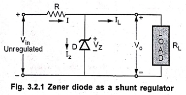
The simplest shunt voltage regulator circuit uses a zener diode, to regulate
the load voltage. Fig. 3.2.1 shows the arrangement of zener diode in a
regulator circuit.
•
The zener diode has a characteristics that as long as the current through it is
between IZmin and IZmax the voltage across it is constant
equal to zener voltage VZ.
•
As zener diode is connected in shunt with the load resistance, the output voltage
is equal to the zener voltage.
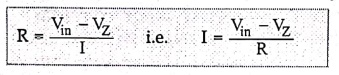
The
value of R can be obtained mathematically as,
R
= [ Vin – VZ ] / I
I
= [ Vin – VZ ] / R
•
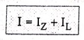
While the relation between the various currents is given by,
I = IZ + IL
Regulation with varying
input voltage:
•
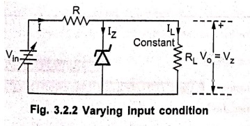
Fig. 3.2.2 shows a zener regulator under varying input voltage condition.
•
It can be seen that the output is
V0 = VZ, is constant.
IL
= V0 / RL = VZ / RL = Constant
•
And I = IZ + IL
•
Now if Vin increases, then the total current I increases. But IL
is constant as VZ is constant. Hence the current IZ
increases to keep IL constant.
•
But as long as IZ is between IZmin and IZmax
the VZ i.e. output voltage V0 is constant.
•
Thus the changes in input voltage get compensated and output is maintained
constant.
•
Similarly if Vin decreases, then current I decreases. But to keep IL
constant, IZ decreass. As long as IZ is between IZmax
and IZmin' the output voltage remains constant.
Regulation with varying
load:
•
Fig. 3.2.3 shows a zener regulator under varying load condition and constant
input voltage.
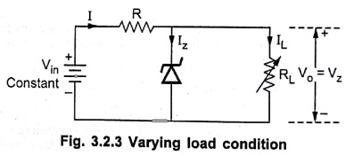
Fig. 3.2.3 Varying load
condition
•
The input voltage is constant while the load resistance RL is
variable.
•
As Vin is constant and V0 = VZ is constant,
then for constant R the current I is constant.
I
= [ Vin ‒ VZ ] / R
constant
= IL + IZ
•
Now if RL decreases so IL increases, to keep I constant IZ
decreases. But as long as it is between IZmin and IZmax
output voltage V0 will be constant.
•
Similarly if RL increases so IL decreases, to keep I
constant IZ increases. But as long as it is between IZmin
and IZmax' output voltage V0 will be constant.
•
Thus irrespective of changes in the line voltage or changes in the load, the
output voltage remains constant.
Design of Zener Regulator
•
Let us see the design of zener regulator with varying load as well as varying
input conditions.
•
Let
VInmin
= Minimum value of input voltage,
Vinmax
= Maximum value of input voltage
ILmax
= Maximum value of load current,
ILmin
= Minimum value of load current
IZmax
= Maximum value of zener current,
IZmin
= Minimum value of zener current
V0 = VZ = Output
voltage
•
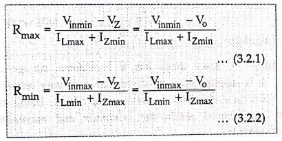
The limiting values series resistance R for a given zener can be obtained as,
•
For any value of R between Rmax and Rmin' the circuit
works successfully as a regulator.
•
If load current or input voltage is constant and not varying then its both
maximum and minimum values must be treated as a constant value in the above
equations, to obtain Rmax and Rmin' The ILmin value
is generally treated to be zero.
•
To satisfy the equations (3.2.1) and (3.2.2), proper zener diode having IZmin
and IZmax values, which can satisfy the required varying load
conditions, must be used in the circuit.
•
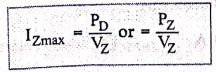
If IZmax is not given, but the power dissipation rating of zener
diode is given then the maximum zener current can be obtained as,
IZmax
= PD / VZ
Or
IZmax
= PZ / VZ
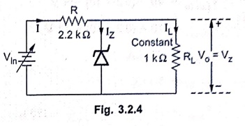
Ex. 3.2.1: For a zener regulator shown in the
Fig. 3.2.4, calculate the range of input voltage for which output will remain
constant.
VZ = 6.1 V, IZmin = 2.5
mA, IZmax = 25 mA, rZ = 0Ω
Solution:
RL = 1 kΩ, VZ = 6.1 V
IL
= VZ / RL = 6.1 / 1×103
= 6.1 mA constant
For
Vin(max) IZ = IZmin = 2.5 mA
I
= IZmin + IL = 2.5 + 6.1 = 8.6 mA
Vin(min)
= VZ + IR
=
6.1 +8.6×10‒3×2.2×103
=
25.02 V
For Vin(max) = Iz = IZmin = 25 mA
I
= IZmin + IL = 25 + 6.1 = 31.1 mA
Vin(max)
= VZ + IR
=
6.1 +31.1×10‒3×2.2×103
=
74.52 V
Thus
the range of input voltage is 25.02 V to 74.52 V, for which output will be
constant.
Ex. 3.2.2: In a zener regulator, the input
D.C. is 10 V ±20%. The output requirements are 5 V, 20 mA. Assuming Izmin
and Iz max as 5 mA and 80 mA.
Design the zener
regulator.
Solution:
V0
= 5V
and
IL = 20 mA
RL
= V0/IL = 5V/20×10‒3
= 250 Ω
The
maximum and minimum values of current limiting resistance can be obtained with,
ILmax
= ILmin = 20 mA
Rmax
= ( Vinmin ‒ V0 ) / ( ILmax + IZmin )
Now
Vinmin
= 10 ‒ (0.2 × 10) = 8 V
Vinmax
= 10+ (0.2 × 10) = 12 V
IZmax
= 80 mA
IZmin
= 5 mA
Rmax
= (8‒5) / (20×10‒3+5x10‒3) = 120 Ω
Rmin
= ( Vinmax ‒ V0 ) / ( ILmin + IZmax )
=
12‒5 / (20×10‒3 + 80×10‒3) = 70 Ω
So
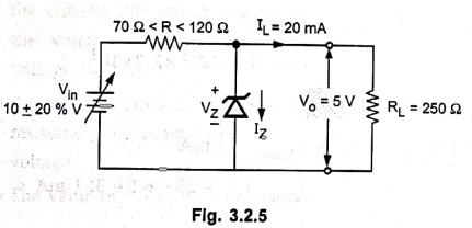
series resistance R must be selected between 70 Ω to 120 Ω. So designed circuit
is as shown in Fig. 3.2.5.
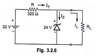
Ex. 3.2.3: A 24 V, 600 mW zener diode is
used for providing a 24 V stabilized supply to a variable load. If the input
voltage is 32 V, calculate
i) The value of series
resistance required ii) Diode current when the load is 1200 Q.
Solution:
V0 = VZ = 24 V
PZ = 600 mW
Vin
= 32 V
IZmax
= PZ/V0 = (600× 10‒3) / 24 = 25 mA
Rmin = (Vinmax ‒ V0)
/ (ILmin + IZmax )
=
(32‒24) / (0 + 25×10‒3)
=
320 Ω
i)
As Vin and IL are not changing, R = Rmin = 320
Ω is sufficient, to work the circuit as regulator
ii)
Now
RL
= 1200 Ω
IL = V0/RL =
24/1200 = 20 mA
while
IT = (Vin ‒ VZ)
/ R = (32‒24) / 320 = 25 mA
IZ = IT‒IL = 25
‒ 20 = 5 mA
As
IZ
= IZmin = 5 mA, circuit will work
Ex. 3.2.4: A zener diode has a breakdown
voltage of 10 V. It is supplied from a voltage source varying between 20 ‒ 40 V
in series with a resistance of 820 Ω. Using an ideal zener model obtain the
minimum and maximum zener currents.
Solution:
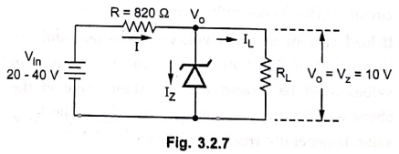
The
circuit is shown in Fig. 3.2.7.
I
= (Vin ‒ V0) / R
I
= (Vin ‒ 10) / 820
Imax
= (Vin(max) ‒ 10) / 820
=
(40‒10) / 820
=
36.585 mA
IZmin
= 0A …. For ideal zerer diode
Now
I = IZ + IL
Imax
= IZmin + ILmax
IL(max)
= Imax = 36.585 mA
when
IL
= IL(min) = 0 A
……… Open load terminals.
Under
this condition if Vin = Vin(max) then,
I = 36.585 mA
and
IZ = IZmax = 36.585 mA
Ex. 3.2.5: Calculate the output ripple
voltage in a zener regulator if the limiting resistance RS = 100 Ω,
zener dynamic resistance rZ = 10 Ω, unregulated input voltage is 12
volts with 2 volts ripple, VZ = 5.6 V and load current is 10 mA.
Solution:
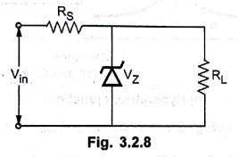
The
circuit is shown in Fig. 3.2.8.
RS
= 100 Ω, rZ = 10 Ω
Vin
= 12 V, ΔVin = 2 V
VZ
= 5.6 V, IL = 10 mA
Now
RL
= VZ/ IL = 5.6 / 10×10‒3 = 560 Ω
When
input ripple voltage is considered, the corresponding output ripple will be
because of rZ. Hence consider equivalent circuit with with ripple AVin
= 2V is applied at input, as shown in Fig. 3.2.8 (a).
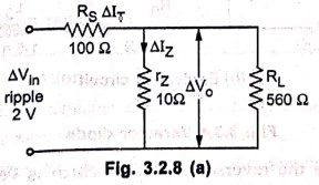
As
input is changing and change in output is to be calculated which is due to rz,
VZ is not considered which is constant.
ΔIT
= ΔVin / [ RS + (rZ||RL) ]
=
2 / [100+(10||560)]
=
18.2108 mA
ΔIZ
= ΔIT × RL/(rZ+RL) = 18.2108 × (
560 / 10+560 )
=
17.89 mA
...Current distribution
ΔV0
= Output ripple voltage = Δ IZ
× rZ
=
17.89×10‒3 ×10 = 178.913 mV
Review
Questions
1. Explain the principle of working of zener diode as a
regulator.
2. Discuss the performance of zener diode regulator interms of
the source and load effects.
Electron Devices: Chapter 3: Special Diodes : Tag: electronics : Working Principle, Construction, Circuit Diagram, Example Solved Problems - Zener Diode as a Shunt Regulator
Electron Devices: Chapter 3: Special Diodes
Under Subject

Electron Devices
EC25C01 2nd Semester ECE Dept | 2025 Regulation | 2nd Semester 2025 Regulation
Related Subjects

English Essentials II
EN25C02 2nd Semester | 2025 Regulation | 2nd Semester 2025 Regulation

Tamils and Technology தமிழர்களும் தொழில்நுட்பமும்
UC25H02 2nd Semester | 2025 Regulation | 2nd Semester 2025 Regulation

Linear Algebra
MA25C02 2nd Semester | 2025 Regulation
Electron Devices
EC25C01 2nd Semester ECE Dept | 2025 Regulation | 2nd Semester 2025 Regulation

Data Structures using CPlusPlus
CS25C05 2nd Semester ECE Dept | 2025 Regulation | 2nd Semester 2025 Regulation

Circuits and Network Analysis
EC25C02 2nd Semester ECE Dept | 2025 Regulation | 2nd Semester 2025 Regulation

Re-Engineering for Innovation
ME25C05 2nd Semester | 2025 Regulation | 2nd Semester 2025 Regulation

Engineering Drawing - Laboratory
ME25C01 2nd Semester | 2025 Regulation | 2nd Semester 2025 Regulation

Data Structures using CPlusPlus - Laboratory
CS25C05 2nd Semester ECE Dept | 2025 Regulation | 2nd Semester 2025 Regulation

Devices and Circuits Laboratory
EC25C03 2nd Semester ECE Dept | 2025 Regulation | 2nd Semester 2025 Regulation