Electron Devices: Chapter 3: Special Diodes
Photodiode
Symbol, Working Principle, Characteristics, Small Signal Model, Advantages, Disadvantages, Applications

Questions: 1. Discuss the working principle of a photodiode. 2. What is photodiode ? Explain its construction and operation. 3. Explain the V‒I characteristics of photodiode. 4. State the advantages, disadvantages and applicaitons of photodiode.
Photodiode
•
The photodiode is a semiconductor p‒n junction device whose region of operation
is limited to the reverse biased region.
•
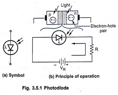
Fig. 3.5.1 (a) shows the symbol of photodiode while Fig. 3.5.1 (b) shows the
working principle of photodiode.
•
The photodiode is connected in reverse biased condition. The depletion region
width is large.
•
Under normal condition, it carries small reverse current due to minority charge
carriers.
•
When light is incident through glass window on the p‒n junction, photons in the
light bombard the p‒n junction and some energy is imparted to the valence
electrons.
•
Due to this, valence electrons are dislodged from the covalent bonds and become
free electrons.
•
Thus more electron‒hole pairs are generated,
•
Thus total number of minority charge carriers increases and hence the reverse
current increases.
1. Photodiode Characteristics
•
The photodiode is designed such that it is sensitive to the light.
•
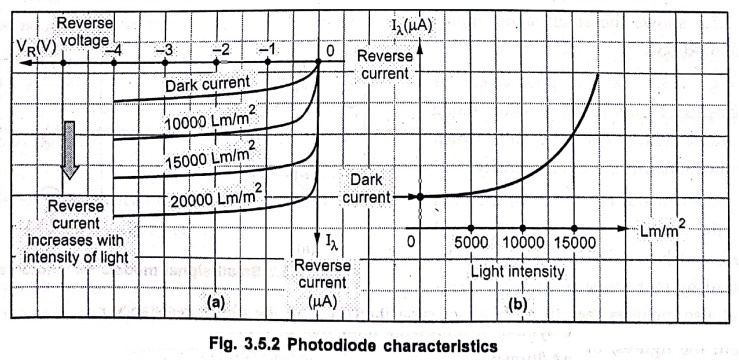
When there is no light, the reverse biased photodiode carries a current which
is very small and called by dark current. It is denoted as Iλ. It is
purely due to thermally generated minority carriers.
•
When light is allowed to fall on a p‒n junction through a small window, photons
transfer energy to valence electrons to make them free. Hence reverse current
increases. It is proportional to the light intensity.
•
Fig. 3.5.2 shows the photodiode characteristics. Fig. 3.5.2 (a) shows the
relation between reverse current and light intensity while Fig. 3.5.2 (b) shows
relation between reverse voltage and reverse current at different light
intensities.
•
It can be seen that reverse current is not dependent on reverse voltage and
totally depends on light intensity.
2. Use of Photodiode as Variable Resistance Device
•
Consider a typical photodiode with dark current Iλ=20 μA at VR=
‒2V
Dark resistance = VR/Iλ
= 2 / 20 μΑ = 100 kΩ
•
If now photodiode is illuminated with 25000 Lm/m2 (Lumens per square
metres) then current changes to 350 μA at same reverse voltage.
Illuminated resistance = 2 / 350 μΑ = 8.914
ΚΩ
•
This shows that the photodiode can be used as a variable resistance device
controlled by light intensity. It is also called photoconductive device.
•
The response of photodiode is very fast hence change in resistance from high to
low or otherwise is also very fast. Hence it can be used in variety of
applications.
3. Why to be used in Reverse Biased?
•
The reverse current without light in diode is in the range of μA. The change in
this current due to the light is also in the range of μA. Thus such a change
can be significantly observed in the reverse current.
•
If the photodiode is forward biased, the current flowing through it is in mA.
The applied forward biased voltage takes the control of the current instead of
the light.
•
The change in forward current due to light is negligible and can not be
noticed.
•
The resistance of forward biased diode is not affected by the light.
•
Hence to have significant effect of light on the current and to operate
photodiode as a variable Kresistance device, it is always connected in reverse
biased condition.
4. Small Signal Model of Photodiode
•
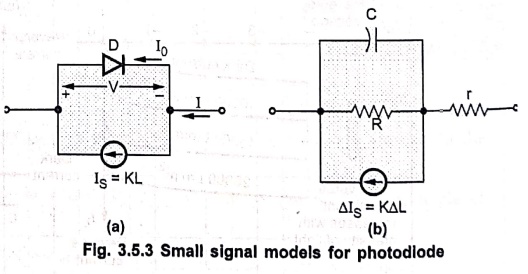
Fig. 3.5.3 shows the small signal model for photodiode.
•
In Fig. 3.5.3 (a) a photodiode is represented by an ideal junction diode in
parallel with a current source which is proportional to the light intensity.
•
The model in the Fig. 3.5.3 (b) assumes that the diode is heavily reversed
biased, and hence that the diode may be replaced by its reverse resistance R.
This model also includes the effect of barrier capacitance C and the ohmic
resistance r.
•
In both the figures, the symbol L represents light flux in lumens, and K is a
proportionality constant in the range 10 to 50 mA/lumen.
5. Advantages
1.
Can be used as variable resistance device.
2.
Highly sensitive to the light.
3.
The speed of operation is very high. The switching of current and hence the
resistance value from high to low or otherwise is very fast.
6. Disadvantages
1.
The dark current Iλ is temperature dependent.
2.
The overall photodiode characteristics are temperature dependent hence have
poor temperature stability.
3.
The current and change in current is in the range of μA which may not be
sufficient to drive other circuits. Hence amplification is necessary.
7. Photodiode Applications
•
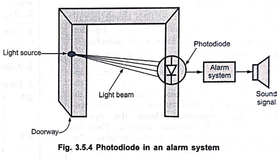
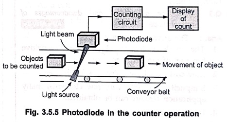
The two commonly used systems using photodiode are alarm system and a counting
ag system. Fig. 3.5.4 shows a photodiode employed in an alarm system.
•
The reverse current Iλ continues to flow as long as light beam is
incident on the photodiode. When the light is interrupted, the current Iλ
drops to the dark current level. This initiates the alarm system sounding the
alarm.
•
Fig. 3.5.5 shows a photodiode used to count the items on a conveyor belt. As
each item passes, the light beam is broken. Thus reverse current Iλ
drops to the dark current level. This activates the counting mechanism and the
counter is increased by one.
•
Other applications of photodiode are
1.
As a cell.
2.
As a variable resistance device.
3.
In light intensity meters.
4.
In high‒speed logic circuits.
5.
In fibre optic receivers.
Review
Questions
1. Discuss the working principle of a photodiode.
2. What is photodiode ? Explain its construction and operation.
3. Explain the V‒I characteristics of photodiode.
4. State the advantages, disadvantages and applicaitons of
photodiode.
Electron Devices: Chapter 3: Special Diodes : Tag: electronics : Symbol, Working Principle, Characteristics, Small Signal Model, Advantages, Disadvantages, Applications - Photodiode
Electron Devices: Chapter 3: Special Diodes
Under Subject

Electron Devices
EC25C01 2nd Semester ECE Dept | 2025 Regulation | 2nd Semester 2025 Regulation
Related Subjects

English Essentials II
EN25C02 2nd Semester | 2025 Regulation | 2nd Semester 2025 Regulation

Tamils and Technology தமிழர்களும் தொழில்நுட்பமும்
UC25H02 2nd Semester | 2025 Regulation | 2nd Semester 2025 Regulation

Linear Algebra
MA25C02 2nd Semester | 2025 Regulation
Electron Devices
EC25C01 2nd Semester ECE Dept | 2025 Regulation | 2nd Semester 2025 Regulation

Data Structures using CPlusPlus
CS25C05 2nd Semester ECE Dept | 2025 Regulation | 2nd Semester 2025 Regulation

Circuits and Network Analysis
EC25C02 2nd Semester ECE Dept | 2025 Regulation | 2nd Semester 2025 Regulation

Re-Engineering for Innovation
ME25C05 2nd Semester | 2025 Regulation | 2nd Semester 2025 Regulation

Engineering Drawing - Laboratory
ME25C01 2nd Semester | 2025 Regulation | 2nd Semester 2025 Regulation

Data Structures using CPlusPlus - Laboratory
CS25C05 2nd Semester ECE Dept | 2025 Regulation | 2nd Semester 2025 Regulation

Devices and Circuits Laboratory
EC25C03 2nd Semester ECE Dept | 2025 Regulation | 2nd Semester 2025 Regulation