Electron Devices: Chapter 3: Special Diodes
Varactor Diode
Symbol, Equivalent Circuit, Applications

Questions: 1. What is varactor diode? How capacitance of a diode varies with reverse voltage? 2. Explain the principle behind the varactor diode and list out its application. 3. Write a note on varactor diode.
Varactor
Diode
•
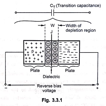
In a normal diode, the depletion region exists between p‒region and n‒region as
shown in the Fig. 3.3.1.
•
The p‒region and n‒region act like the plates of capacitor while the depletion
region acts like dielectric,
•
Thus there exists a capacitance at the p‒n junction called transition
capacitance, space charge capacitance, barrier capacitance or depletion region
capacitance. It is denoted as CT.
•
Mathematically it is given by the expression,
Ст = εΑ / W
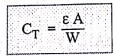
where
ε
= Permittivity of semiconductor,
A
= Area of cross section
W
= Width of depletion region
•
As the reverse biased applied to the diode increases, the width of the
depletion region (W) increases. Thus the transition capacitance CT
decreases.
•
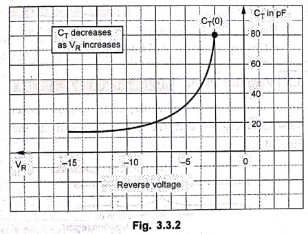
In short, the capacitance can be controlled by the applied voltage. The
variation of CT with respect to the applied reverse bias voltage is
shown in Fig. 3.3.2.
•
As reverse voltage is negative, graph is shown in the second quadrant.
•
For a particular diode shown, CT varies from 80 pF to less than 5 pF
as VR changes from 2 V to 15 V.
•
In practice, special type of diodes are manufactured which shows the transition
capacitance property more predominantly as compared to the normal diodes. Such
diodes are called varactor diodes, varicap, (VVC (Voltage Variable
Capacitance)), or tuning diodes.
•
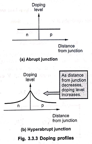
The doping profile of some varactor diodes is hyperabrupt. It means that the
doping level increases towards the junction. This produces very narrow
depletion region and large capacitive effect.
•
The capacitance vary more dominantly with reverse voltage in such diodes. The
doping profiles for abrupt and hyperabrupt junction are shown in Fig. 3.3.3.
1. Symbol and Equivalent Circuit
•
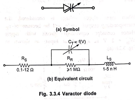
Fig. 3.3.4 (a) shows the symbol of varactor diode while Fig. 3.3.4 (b) shows
the first approximation for its equivalent circuit in the reverse bias region.
•
The RR is the reverse resistance which is very large while RS
is the geometric resistance of diode which is very small. The inductance LS
indicates that there is a high frequency limit associated with the use of
varactor diodes.
2. Applications
•
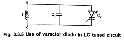
Fig. 3.3.5 shows how varactor diode can be connected in a LC tuned circuits.
•
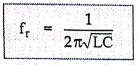
The resonance frequency for a parallel LC tuned circuit is given by,
fr = 1 / 2π√(LC)
•
As varactor diode is connected in parallel, the resultant capacitance becomes C1+C2.
•
Hence the resonance frequency becomes,
fr= 1 / 2π/√[L(C1+C2)]
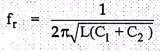
where
C2 is transistion capacitance of varactor diode
•
The value of C2 can be changed by controlling the voltage applied to
the circuit. Hence circuit can be tuned by changing voltage applied at a
resonance frequency, this is called electrical tuning.
•
The various other applications of varactor diodes are,
1.
Tuned circuits
2.
FM modulators
3.
Automatic frequency control devices
4.
Adjustable bandpass filters
5.
Parametric amplifiers
6.
Television receivers
Review
Questions
1. What is varactor diode? How capacitance of a diode varies
with reverse voltage?
2. Explain the principle behind the varactor diode and list out
its application.
3. Write a note on varactor diode.
Electron Devices: Chapter 3: Special Diodes : Tag: electronics : Symbol, Equivalent Circuit, Applications - Varactor Diode
Electron Devices: Chapter 3: Special Diodes
Under Subject

Electron Devices
EC25C01 2nd Semester ECE Dept | 2025 Regulation | 2nd Semester 2025 Regulation
Related Subjects

English Essentials II
EN25C02 2nd Semester | 2025 Regulation | 2nd Semester 2025 Regulation

Tamils and Technology தமிழர்களும் தொழில்நுட்பமும்
UC25H02 2nd Semester | 2025 Regulation | 2nd Semester 2025 Regulation

Linear Algebra
MA25C02 2nd Semester | 2025 Regulation
Electron Devices
EC25C01 2nd Semester ECE Dept | 2025 Regulation | 2nd Semester 2025 Regulation

Data Structures using CPlusPlus
CS25C05 2nd Semester ECE Dept | 2025 Regulation | 2nd Semester 2025 Regulation

Circuits and Network Analysis
EC25C02 2nd Semester ECE Dept | 2025 Regulation | 2nd Semester 2025 Regulation

Re-Engineering for Innovation
ME25C05 2nd Semester | 2025 Regulation | 2nd Semester 2025 Regulation

Engineering Drawing - Laboratory
ME25C01 2nd Semester | 2025 Regulation | 2nd Semester 2025 Regulation

Data Structures using CPlusPlus - Laboratory
CS25C05 2nd Semester ECE Dept | 2025 Regulation | 2nd Semester 2025 Regulation

Devices and Circuits Laboratory
EC25C03 2nd Semester ECE Dept | 2025 Regulation | 2nd Semester 2025 Regulation