Electron Devices: Chapter 3: Special Diodes
Special Diodes: Two Marks Important Questions and Answers
Electron Devices
Electron Devices: Chapter 3: Special Diodes: Anna University Part A Two Marks Important Questions and Answers
Electron
Devices:
Chapter 3: Special Diodes
Two Marks
Questions with Answers
1. What is tunneling effect
in diodes ?
In
tunnel diode, p and n regions are very heavily doped. Due to this, width of the
depletion region reduces considerably.
In
normal p‒n junction, the width of the depletion region is about 5 × 10⁻⁴
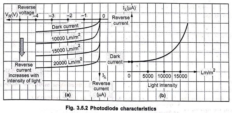
cm while in tunnel diode it is about 1 × 10‒6 cm which is about
1/100th of normal diode.
Due
to such a thin depletion region, the charge carriers i.e. electrons can easily
penetrate the depletion region due to their high kinetic energy. This
penetration of electrons through the depletion region due to high velocities is
called tunneling
2. What is negative
resistance in tunnel diode ?
In
tunnel diode characteristics, the slope dI/dV becomes zero at the peak point.
If the forward voltage is increased further beyond the peak voltage Vp, then
current starts decreasing rather than increasing. Hence the dynamic conductance
dI/dV becomes negative. Thus the dynamic resistance dV/dI is also negative.
This region is called neagative resistance region in tunnel diode.
3. State the advantages and
disadvantages of tunnel diode.
The
advantages are,
1.
The peak point (VP,IP) is not sensitive function of
temperature.
2.
Low cost
3.
Low noise
4.
High speed
5.
Simplicity i.e. with very few elements, many application circuits can be
obtained.
6.
Low power consumption.
The
disadvantages are,
1.
Low output voltage swing.
2.
No isolation between input and output.
4. State the applications
of tunnel diode.
1.
As a high speed switch
2.
In pulse and digital circuits.
3.
In switching networks.
4.
In negative resistance oscillators.
5.
In timing and computer logic circuitry.
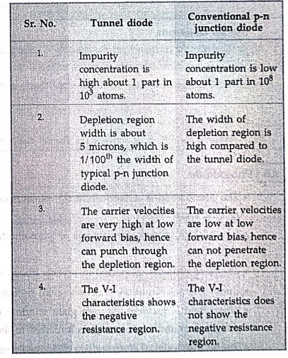
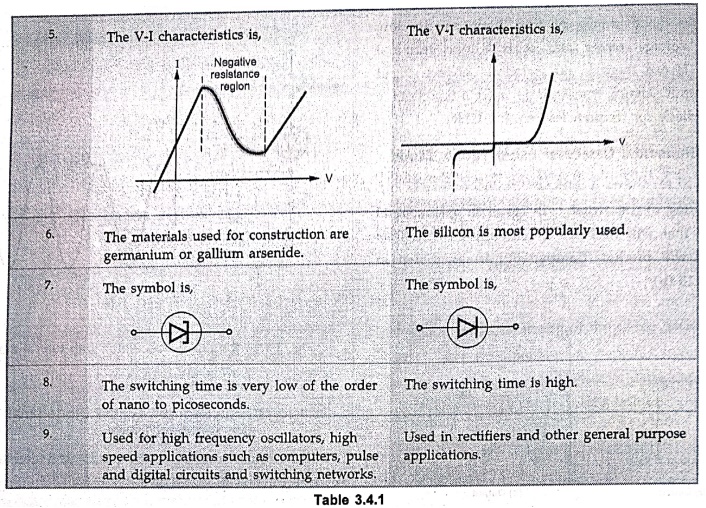
5. State the comparison
between tunnel diode and conventional diode.
Tunnel diode
1. Impurity concentration is high about 1 part in 103 atoms.
2. Depletion region width is about 5 microns, which is 1/100th the width of typical p‒n junction diode.
3. The carrier velocities are very high at low forward bias, hence can punch through the depletion region.
4. The V‒I characteristics shows the negative resistance region.
Conventional p‒n junction diode
1. Impurity concentration is low about 1 part in 108 atoms.
2. The width of depletion region is high compared to the tunnel diode.
3. The carrier velocities are low at low forward bias, hence can not penetrate the depletion region.
4. The V‒I characteristics does not show the negative resistance region.
6. What is the feature of
varactor diode ?
When
reverse biased, the varactor diode shows a dominant transition capacitance.
This capacitance decreases as reverse voltage increases. Thus varactor diode
shows voltage variable capacitance characteristics when reverse biased.
7. State the applications
of varactor diode.
1.
Tuned circuits
2.
FM modulators
3.
Automatic frequency control devices
4.
Television receivers.
5.
Adjustable bandpass filters
6.
Parametric amplifiers.
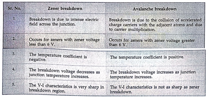
8. Compare Zener breakdown
and avalanche breakdown in Zener diode.
Zener breakdown
1. Breakdown is due to intense electric field across the junction.
2. Occurs for zeners with zener voltage less than 6 V.
3. The temperature coefficient is negative.
4. The breakdown voltage decreases as junction temperature increases.
5. The V‒I characteristics is very sharp in breakdown region.
Avalanche breakdown
1. Breakdown is due to the collision of accelerated charge carriers with the adjacent atoms and due to carrier multiplication.
2. Occurs for zeners with zener voltage greater than 6 V
3. The temperature coefficient is positive.
4. The breakdown voltage increases as junction temperature increases.
5. The V‒1 characteristics is not as sharp as zener breakdown.
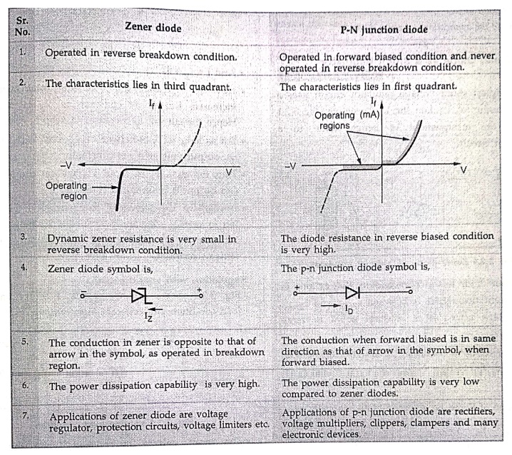
9. Compare Zener diode with
conventional diode.
Zener diode
1. Operated in reverse breakdown condition.
2. The characteristics lies in third quadrant.
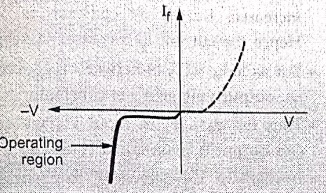
3. Dynamic zener resistance is very small in reverse breakdown condition.
4. Zener diode symbol is, 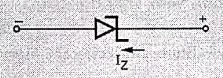
5. The conduction in zener is opposite to that of arrow in the symbol, as operated in breakdown region.
6. The power dissipation capability is very high.
7. Applications of zener diode are voltage regulator, protection circuits, voltage limiters etc.
P‒N junction diode
1. Operated in forward biased condition and never operated in reverse breakdown condition.
2. The characteristics lies in first quadrant.
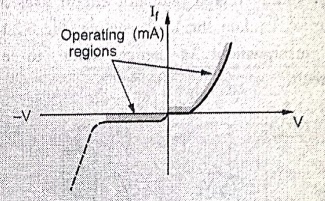
3. The diode resistance in reverse biased condition is very high.
4. The p‒n junction diode symbol is, 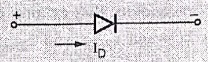
5. The conduction when forward biased is in same direction as that of arrow in the symbol, when forward biased.
6. The power dissipation capability is very low compared to zener diodes.
7. Applications of p‒n junction diode are rectifiers, voltage multipliers, clippers, clampers and many electronic devices.
10. Mention the applications
of Zener diode.
1.
As a voltage regulating element in regulators
2.
In various protection circuits
3.
In clipping circuits
11. What is temperature
coefficient of a Zener diode ?
The
percentage change in the Zener voltage VZ for every °C change in temperature
is called temperature coefficient of a Zener diode. It is denoted as TC and
expressed as % / °C. Mathematically it can be defined as,
TC
= { ΔVZ / [VZ (Ti‒T0)] } × [100%]
%/°C

where
T1 is the final temperature of junction while T0 is
generally 25 °C at which nominal Zener voltage VZ is specified.
12. What is avalanche
breakdown?
When
reverse voltage is increased, the velocity of minority charge carriers
increases. In such highly accelerated charge carrier collides against electron
involved in covalent bond, then it breaks the covalent bond and electron‒hole
pair. These secondary particles also accelerate and involve in the further
collisions to produce more electron‒hole pairs. This is called carrier
multiplication. Due to such large number of charge carriers breakdown of
junction takes place. Such a breakdown is called avalanche breakdown.
13. Define work function
for a material.
It
is defined as the amount of minimum energy required to remove an electron from
a material to a point in the vacuum immediately outside the material surface.
14. What is voltage
regulator?
The
voltage regulator is a circuit which keeps the output voltage constant inspite
of changes in load current or input voltage.
15. What are the
limitations of using Zener diode regulator?
1.
The maximum load current that can be supplied is limited to [IZmax ‒
IZmin ].
2.
A large amount of power is wasted in the zener diode and the series resistance
R, in comparison with the load power.
3.
The stability factor and the output resistance are not very low, as desired for
a regulator circuit.
16. What is dark current ?
When
there is no light falling on photodiode, as it is connected in reverse biased,
it carries very small reverse current which is called dark current.
17. Draw the
characteristics of photodiode.
18. Why photodiode is used
in reverse biased condition ?
The
reverse current of photodiode is very small and the change in the current due
to the light is also very small. Thus this small change can be noticed when the
photodiode is in reverse biased condition. It is connected in forward biased
condition, it will carry large current and the small change in the current due
to light can not be significant in such a forward current. Also its resistance
in forward biased condition is not affected by light. Hence to have significant
effect of the light on the operation, photodiode is connected in reverse biased
condition.
20. State the advantages
and disadvantages of photodiode.
Advantages
1. Can be used as variable resistance device.
2. Highly sensitive to the light.
3. The speed of operation is very high. The switching of current and hence the resistance value from high to low or otherwise is very fast.
Disadvantages
1. The dark current Iλ is temperature dependent.
2. The overall photodiode characteristics are temperature dependent hence have poor temperature stability.
3. The current and change in current is in the range of μA which may not be sufficient to drive other circuits. Hence amplification is necessary.
21. State the applications
of photodiode.
1.
Alarm system
2.
Counting system
3.
As a cell
4.
As a variable resistance device
5.
In light intensity meters
6.
In high speed logic circuits
7.
In fibre optic receivers
Electron Devices: Chapter 3: Special Diodes : Tag: electronics : Electron Devices - Special Diodes: Two Marks Important Questions and Answers
Electron Devices: Chapter 3: Special Diodes
Under Subject

Electron Devices
EC25C01 2nd Semester ECE Dept | 2025 Regulation | 2nd Semester 2025 Regulation
Related Subjects

English Essentials II
EN25C02 2nd Semester | 2025 Regulation | 2nd Semester 2025 Regulation

Tamils and Technology தமிழர்களும் தொழில்நுட்பமும்
UC25H02 2nd Semester | 2025 Regulation | 2nd Semester 2025 Regulation

Linear Algebra
MA25C02 2nd Semester | 2025 Regulation
Electron Devices
EC25C01 2nd Semester ECE Dept | 2025 Regulation | 2nd Semester 2025 Regulation

Data Structures using CPlusPlus
CS25C05 2nd Semester ECE Dept | 2025 Regulation | 2nd Semester 2025 Regulation

Circuits and Network Analysis
EC25C02 2nd Semester ECE Dept | 2025 Regulation | 2nd Semester 2025 Regulation

Re-Engineering for Innovation
ME25C05 2nd Semester | 2025 Regulation | 2nd Semester 2025 Regulation

Engineering Drawing - Laboratory
ME25C01 2nd Semester | 2025 Regulation | 2nd Semester 2025 Regulation

Data Structures using CPlusPlus - Laboratory
CS25C05 2nd Semester ECE Dept | 2025 Regulation | 2nd Semester 2025 Regulation

Devices and Circuits Laboratory
EC25C03 2nd Semester ECE Dept | 2025 Regulation | 2nd Semester 2025 Regulation