Electron Devices: Chapter 3: Special Diodes
Tunnel Diodes
Construction, Tunneling Effect, Energy Band Structure, Working Principle, Load Line, Characteristics, Symbol, Advantages, Applications, Comparison

Questions: 1. Describe the construction, the symbol, V‒I characteristics and applications of tunnel diode. 2. With energy band diagram, explain the theory and characteristics of tunnel diode. 3. Write short note on tunnel diode. 4. What is the difference between the Tunnel diode and ordinary PN diode ?. Tunnel Diodes: 1. Construction 2. Tunneling Effect 3. Energy Band Structure of Tunnel Diode 4. Working Principle 5. Load Line for Tunnel Diode 6. Characteristics and Symbol 7. Advantages of Tunnel Diode 8. Sinusoidal Oscillator using Tunnel Diode 9. Other Applications of Tunnel Diode 10. Comparison of Tunnel Diode and Conventional Diode
Tunnel
Diodes
•
A normal p‒n junction has an impurity concentration of about 1 part in 108.
This much amount of doping has the depletion layer width of about 5 microns
i.e. 5×10‒4 cm.
•
The diodes in which the concentration of impurity atoms is greatly increased
upto 1 part in 103, to get completely changed characteristics, are
called tunnel diodes. These diodes are first introduced by Leo Esaki in 1958.
1. Construction
•
The most common commercially available tunnel diodes are made from the
germanium or gallium arsenide.
•
The basic construction of an advanced design tunnel diode is shown in Fig.
3.4.1.
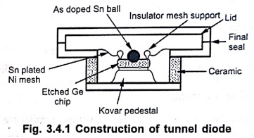
Fig. 3.4.1 Construction
of tunnel diode
2. Tunneling Effect
•
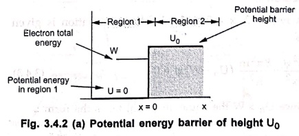
Let us consider an electron of total energy W (joules) moves in region 1, where
the potential energy may be taken as zero, U = 0. At x = 0, there is a
potential energy barrier of height U0 and U0 is greater
than W. This is illustrated in Fig. 3.4.2 (a).
•
Two regions, region 1 and region 2 having two different potential energy are
shown separately in Fig. 3.4.2, and it is important to note that the potential
energy remains constant in region 2 for x > 0. Now we apply the schrödinger
equation for region 1 and region 2 to find the possibility that an electron
will penetrate through the barrier.
Region 1:
Schrödinger
equation is given as
d2Ψ/dx2
+ (8π2m/ h2)WΨ = 0
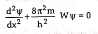
……….. (3.4.1)
For
region 1 it takes the form:
Ψ
= Cε±j(8π2mW/h2)1/2x
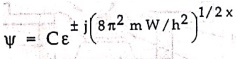
……….(3.4.2)
where
C is a constant.
•
The product of Ψ and its complex conjugate Ψ* gives the probability of finding
an electron between x and x + dx. Since ΨΨ* = |Ψ|2 = C2 =
Constant, the electron has an equal probability of being found anywhere in the
region 1. In other words, the electron is free to move in a region of zero
potential energy.
Region 2:
In
region 2, x > 0 and schrödinger equation is given as
d2Ψ/dx2
– 8π2m/ h2(U0-W)Ψ = 0
……….. (3.4.3)
Since
U0 > W the equation (3.4.3) takes the form :
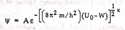
= A ɛ-x/2 d0
…………. (3.4.4)
where
A
constant and
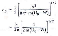
The
solution of equation (3.4.3) is actually of the form
Ψ= Aε-x/2do +B εx/2do
………… (3.4.6)
•
However, B = 0, since it is required that Ψ be finite energy where in the
region 2. Again having the product of Ψ and its complex conjugate Ψ* to find
the probability of the electron between x and x + dc in region 2 we have
ΨΨ* = A2ε-x/do
………... (3.4.7)
•
From equation (3.4.7) we can observe following points.
An
electron can penetrate a potential‒energy barrier.
The
probability of penetrating a potential barrier by electron decreases
exponentially with distance into the barrier region.
•
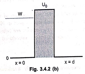
Consider that the potential energy hill has a finite thickness d as shown in
Fig. 3.4.2 (b). Then x = d and equation (3.4.8) becomes
ΨΨ*
= A2ε-d/do
………... (3.4.8)
•
Now, if
1.
d >> d0: The probability that the electron will tunnel through
the barrier is virtually zero.
2.
d→d0 (d approaches d0): A2ε-d/do
becomes large enough to represent an appreciable number of electrons which have
tunneled through the hill.
3. Energy Band Structure of Tunnel Diode
•
We have seen that to achieve tunneling barrier, depth d should approach d0.
However, it is not the only condition to achieive tunneling. It is also
required that occupied energy states exist on the side from which the electron
tunnels and that allowed empty energy level. Hence we will now see the energy
band structure when the impurity concentration is very high.
•
We have seen that in the energy band structure for the lightly doped p‒n diode,
the fermi level Ef lies inside the forbidden energy gap. In the
heavily doped p‒n diode Ef lies outside the forbidden band.
We
know that
Ef = EC ‒ kT In [NC/ND] ……… (3.4.9)
•
For a lightly doped semiconductor, ND <NC, so that
In(NC/ND) is a positive number. Hence EF <EC,
and the fermi level lies inside the forbidden band. For highly doped
semiconductor donor concentrations are more so that ND >NC
and InNC/ND is
negative number. Hence EF > EC, and the fermilevel
lies outside the forbidden band.
•
For the similar reason, for heavily doped F region, NA >NV,
and the fermi‒level lies in the valence band.
We
have,
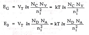
•
When we compare above two equations for heavily doped p‒n diode we find that E0
> EG. Therefore, the contact difference of potential energy E0 exceeds the forbidden
energy gap voltage EG. Hence, at open circuit condition the band
structure for heavily doped p‒n junction is as shown in Fig. 3.4.3.
•
As shown in Fig. 3.4.3, at open circuit, the fermi level in the p‒side is at
the same energy as the fermi level Ef in the n‒side. It is important
that there are no filled states on one side of the junction which are at the
same energy as empty allowed states on the other side. Hence, at open circuit,
there can be no flow of charge in either direction across the junction and the
current is zero.
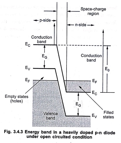
Fig. 3.4.3 Energy band
in a heavily doped p‒n diode under open circuited condition
•
When reverse bias is applied, the height of the barrier is increased above the
open circuit value E0. Hence the n‒side levels must shift downwards
with respect to the p‒side levels, as shown in Fig. 3.4.4. Looking at Fig.
3.4.4, we can notice that there are some energy states (portion in dark black
colour) in the valence band of the p‒side which lie at the same level as
allowed empty states in the conduction band of the n‒side.
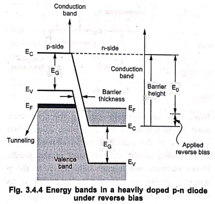
Fig. 3.4.4 Energy bands
In a heavily doped p‒n diode under reverse bias
Hence
these electrons will tunnel from the p to the n‒side, giving rise to a reverse
diode current. As the reverse bias increases, the portion in dark black colour
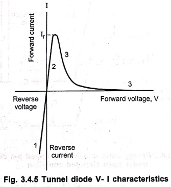
increases, causing the reverse current to increase, as shown in section 1 of
Fig. 3.4.5.
•
When forward bias is applied to the diode the barrier potential E0
decreases. Hence the n‒side levels must shift upward with respect to those on
the p‒side. This is illustrated in Fig. 3.4.6.
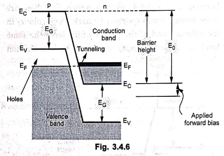
•
Now, there are occupied states in the conduction band of the n‒material (the
dark black colour area) which are at the same energy as allowed empty states
(holes) in the valence band of the p‒side. Hence electrons will tunnel from the
n to the p material, giving rise to the forward current as shown in section 2
of Fig. 3.4.5.
•
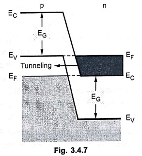
As the forward bias is increased further, n‒side level shifts further upward,
as shown in Fig. 3.4.7. In this situation the maximum number of electrons can
leave occupied states on the left side, giving rise to the peak current IP.
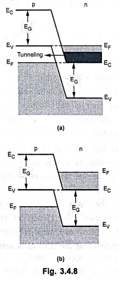
If still more forward bias is applied, the situation shown in Fig. 3.4.8 (a)
exists and the tunneling current decreases, giving rise to section 3 of Fig.
3.4.5.
•
Finally, at an even larger forward bias, the band structure of Fig. 3.4.8 (b)
is obtained. Since now there are no empty allowed states on one side of the
junction at the same energy as occupied states on the other side, the tunneling
current drops to zero. This is illustrated in Fig. 3.4.5.
4. Working Principle
•
In tunnel diode, p and n regions are very heavily doped. Due to this, width of
the depletion region reduces considerably.
•
In normal p‒n junction, the width of the depletion region is about 5 × 10‒4
cm while in tunnel diode it is about 1 × 10‒6 cm which is about
1/100th of normal diode.
•
Due to such a thin depletion region, the charge carriers i.e. electrons can
easily penetrate the depletion region due to their high kinetic energy.
•
This penetration of electrons through the depletion region due to high
velocities is called tunneling and the diode is called tunnel diode. This
happens at very low forward bias voltages.
•
Due to tunneling effect, the tunnel diode shows a negative resistance region.
5. Load Line for Tunnel Diode
•
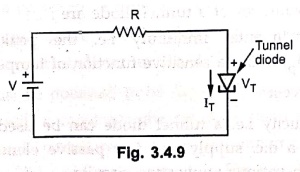
Consider a circuit as shown in Fig. 3.4.9. The supply voltage is V and R is the
load resistance.
•
The drop across the tunnel diode is VT. Applying KVL,
V = ITR + VT
IT = (‒1/R)VT + V/R
………. (3.4.10)
•
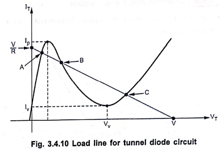
So when IT = 0, VT = V while when VT = 0, IT
= V/R.
Using
these two points a load line can be obtained on V‒I characteristics of tunnel
diode as shown in Fig. 3.4.10.
•
The load line intersects the characteristics at the three points A, B and C.
The load line position and the slope is completely dependent on the network
elements and tunnel diode characteristics.
•
The points A and C are stable operating points as located in positive resistance
region of characteristics. While point B is in the negative resistance region
and hence unstable operating point.
•
An important point regarding stable points A and C is that if there is slight
change in the network conditions there will not be any change in the circuit
behaviour and position of Q point for the circuit. If supply voltage increases
then point C will move up on the curve as voltage across diode VT
will increase. When voltage decreases to original value, point C will regain
its original position back.
•
But if operating point is defined at point B in the unstable region and if
supply voltage slightly increases then correspondingly VT increases
but IT decreases due to negative resistance characteristics. This
further reduces VT and process continues till point shifts into
stable region at point C. If supply voltage slightly decreases, point B moves
up to achieve stable point A.
•
Thus point B can be defined as an operating point using load line concept but
in practice it will get stabilized at the locations A or C.
•
This concept is used in a negative resistance oscillator using a tunnel diode.
6. Characteristics and Symbol
•
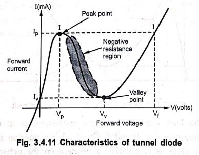
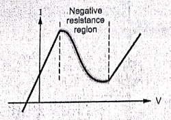
Fig. 3.4.11 shows the volt‒ampere characteristics of a tunnel diode.
•
For small forward voltages (upto 50 mV for germanium) the resistance remains
small, of the order of 5 Ω and current increases.
•
The current attains a peak value IP corresponding to the voltage VP
which is about 600 mV. The IP can vary from few micro amperes to
several hundred amperes.
•
At the peak point, the slope dI/dV of the characteristics becomes zero.
•
If now the forward voltage is increased further, beyond Vp, then the
current starts decreasing rather than increasing. Thus the dynamic conductance
dl/dV becomes negative..
•
Hence the dynamic resistance dV/dI is negative and it shows negative resistance
characteristics. This negative resistance continues till a voltage VV
called valley voltage.
•
At the valley voltage VV, the current is IV and slope
dI/dV becomes again zero.
•
After VV, if the voltage is increased, the current again increases.
Thus resistance again becomes positive and remains positive thereafter.
•
At the so called peak forward voltage Vf, the current again reaches
the value equal to peak current IP.
•
The value of current between IP and IV can be obtained
with three different voltage values. For the value of current between IP
and IV, the characteristics is triple valued.
•
This multivalued feature makes the tunnel diode useful in the pulse and digital
circuits.
•
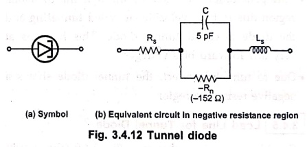
The circuit symbol of a tunnel diode is shown in Fig. 3.4.12 (a) while its
equivalent circuit in the negative resistance region is shown in Fig. 3.4.12
(b).
•
The negative resistance ‒ Rn has a minimum at the point of
inflection between IP and IV.
•
The series resistance RS is due to ohmic contact resistance.
•
The series inductance LS depends upon the lead length and the
geometry of the diode package.
• The junction capacitance C depends upon the bias represents the junction diffusion capacitance and is usually measured at the valley point.
7. Advantages of Tunnel Diode
•
The advantages of a tunnel diode are:
1.
Environmental immunity i.e. the peak point (VP, IP) is
not a sensitive function of temperature.
2.
Low cost.
3.
Simplicity i.e. a tunnel diode can be used along with a d.c. supply and few
passive elements to obtain various application circuits.
4.
Low noise.
5.
High speed i.e. the tunneling takes place at the speed of light hence the
switching times of the order of a nanosecond are easily obtained and switching
times as low as 50 psec also can be obtained.
6.
Low power consumption.
•
The only disadvantage of this diode are its low output voltage swing and it is
a two terminal device. Hence there is no isolation between input and output.
Hence transistor is used along with a tunnel diode for frequencies below 1 GHz.
8. Sinusoidal Oscillator using Tunnel Diode
•
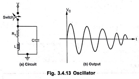
Fig. 3.4.13 (a) shows a tank circuit and a switch.
•
The closing of the switch will result in a sinusoidal voltage that will
decrease in amplitude with time. Thus it will produce damped output as shown in
Fig. 3.4.13 (b).
•
The damping of the oscillator output is due to the dissipative characteristics
of the resistive elements in the tank circuit.
•
The dissipative characteristics of the resistance must be compensated to
produce pure sinusoidal output.
•
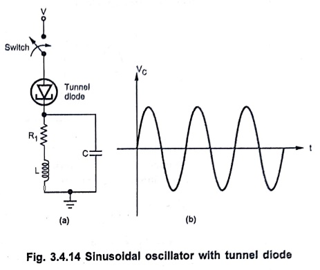
A tunnel diode can be placed in series with the tank circuit as shown in Fig.
3.4.14 (a).
•
It must be operated in its negative resistance region. This will compensate the
resistive characteristics of the tank circuit to produce the undamped purely
sinusoidal response as shown in Fig. 3.4.14 (b).
9. Other Applications of Tunnel Diode
•
The various other applications of tunnel diode are,
1.
As a high speed switch.
2.
In pulse and digital circuits.
3.
In negative resistance and high frequency (microwave) oscillator.
4.
In switching networks.
5.
In timing and computer logic circuitry.
6.
Design of pulse generators and amplifiers.
10. Comparison of Tunnel Diode and Conventional Diode
•
The comparison of tunnel diode and conventional p‒n junction diode is given
below.
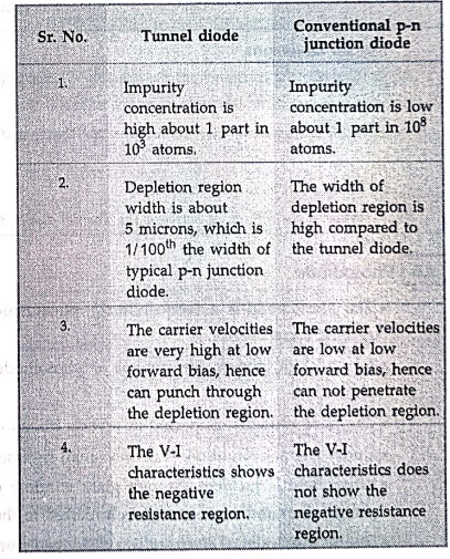
Tunnel
diode
1.
Impurity concentration is high about 1 part in 103 atoms.
2.
Depletion region width is about 5 microns, which is 1/100th the width of
typical p‒n junction diode.
3.
The carrier velocities are very high at low forward bias, hence can punch
through the depletion region.
4.
The V‒I characteristics shows the negative resistance region.
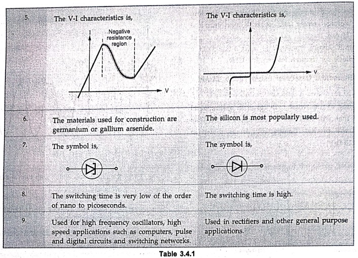
5.
The V‒I characteristics is,
6.
The materials used for construction are germanium or gallium arsenide.
7.
The symbol is, 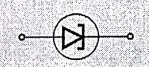
8.
The switching time is very low of the order of nano to picoseconds.
9.
Used for high frequency oscillators, high speed applications such as computers,
pulse and digital circuits and switching networks.
Conventional
p‒n junction diode
1.
Impurity concentration is low about 1 part in 108 atoms.
2.
The width of depletion region is high compared to the tunnel diode.
3.
The carrier velocities are low at low forward bias, hence can not penetrate the
depletion region.
4.
The V‒I characteristics does not show the negative resistance region.
5.
The VI characteristics is,
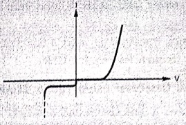
6.
The silicon is most popularly used.
7.
The symbol is, 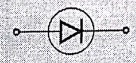
8.
The switching time is high.
9.
Used in rectifiers and other general purpose applications.
Review Questions
1. Describe the construction, the symbol, V‒I characteristics
and applications of tunnel diode.
2. With energy band diagram, explain the theory and
characteristics of tunnel diode.
3. Write short note on tunnel diode.
4. What is the difference between the Tunnel diode and ordinary
PN diode ?
Electron Devices: Chapter 3: Special Diodes : Tag: electronics : Construction, Tunneling Effect, Energy Band Structure, Working Principle, Load Line, Characteristics, Symbol, Advantages, Applications, Comparison - Tunnel Diodes
Electron Devices: Chapter 3: Special Diodes
Under Subject

Electron Devices
EC25C01 2nd Semester ECE Dept | 2025 Regulation | 2nd Semester 2025 Regulation
Related Subjects

English Essentials II
EN25C02 2nd Semester | 2025 Regulation | 2nd Semester 2025 Regulation

Tamils and Technology தமிழர்களும் தொழில்நுட்பமும்
UC25H02 2nd Semester | 2025 Regulation | 2nd Semester 2025 Regulation

Linear Algebra
MA25C02 2nd Semester | 2025 Regulation
Electron Devices
EC25C01 2nd Semester ECE Dept | 2025 Regulation | 2nd Semester 2025 Regulation

Data Structures using CPlusPlus
CS25C05 2nd Semester ECE Dept | 2025 Regulation | 2nd Semester 2025 Regulation

Circuits and Network Analysis
EC25C02 2nd Semester ECE Dept | 2025 Regulation | 2nd Semester 2025 Regulation

Re-Engineering for Innovation
ME25C05 2nd Semester | 2025 Regulation | 2nd Semester 2025 Regulation

Engineering Drawing - Laboratory
ME25C01 2nd Semester | 2025 Regulation | 2nd Semester 2025 Regulation

Data Structures using CPlusPlus - Laboratory
CS25C05 2nd Semester ECE Dept | 2025 Regulation | 2nd Semester 2025 Regulation

Devices and Circuits Laboratory
EC25C03 2nd Semester ECE Dept | 2025 Regulation | 2nd Semester 2025 Regulation