Electron Devices: Chapter 3: Special Diodes
Zener diode
Construction, Symbol, Breakdown Mechanisms, VI Characteristics, Equivalent Circuit Diagram, Ratings, Comparison, Applications

Questions: 1. Explain the breakdown mechanisms in zener diode. 2. Distinguish between zener and avalanche breakdown. 3. Draw the VI characteristics of zener diode and explain its operation. 4. Explain the dynamic resistance and equivalent circuit of a zener diode. 5. Explain the zener diode parameters. 6. Compare zener diode and the conventional p‒n unction diode. 7. State the applications of zener diode. . Index: i. Breakdown Mechanisms in Zener Diode, ii. V‒I Characteristics of Zener Diode, ii. Equivalent Circuit of a Zener Diode, iii. Zener Diode Ratings, iv. Comparison of Zener Diode and Conventional Diode, v. Applications of Zener Diode
Zener
diode
•
A zener diode is a silicon p‒n junction semiconductor device which is operated
in its reverse breakdown region.
•
The zener diodes are fabricated with precise breakdown voltages by controlling
the doping level during manufacturing.
•
When reverse biased, if the reverse current of zener diode is limited using a
series resistance then the power dissipation at the junction is limited to such
a level which will not damage the diode and the zener diode continues to
operate safely in reverse breakdown region.
•
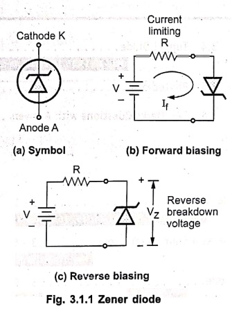
Fig. 3.1.1 (a) shows the symbol of zener diode. Fig. 3.1.1 (b) shows the
forward biasing of zener diode. It acts similar to the conventional diode in
forward biased. Fig. 3.1.1 (c) shows the reverse biasing of zener diode. But in
reverse biased, it is operated in reverse breakdown region.
1. Breakdown Mechanisms in Zener Diode
•
In zener diode there are two distinct mechanisms due to which breakdown occurs.
1. Zener breakdown:
When reverse voltage is less than 6 V, there exists an intense electric field
across the p‒n junction. Due to this, high force is exerted on the valence
electrons of atoms, tending to separate them from respective nuclei. Thus large
electron‒hole pairs are generated due to which there is a reverse breakdown,
causing large current to flow.
2. Avalanche breakdown:
When reverse voltage is greater than 6 V, the minority charge carriers
accelerate. There are collisions between these carriers and electrons involved
in the covalent bonds of the crystal. Due to this collision, the valence
electron in covalent bond becomes free and accelerate. This further collides
with another valence electron to make it free. This is called carrier
multiplication. This action is very fast to generate large electron‒hole pairs
and breakdown occurs.
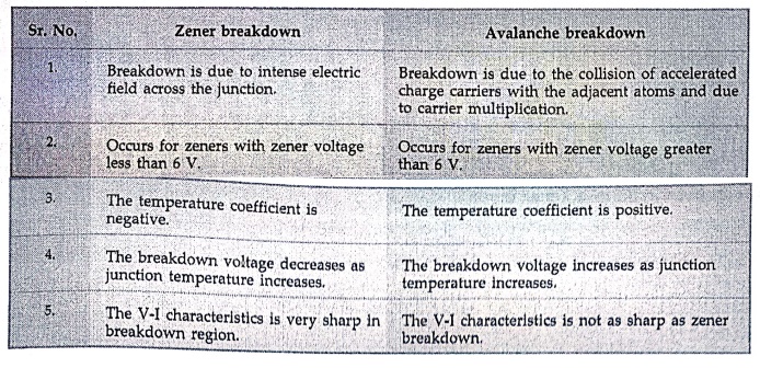
Zener breakdown
1.
Breakdown is due to intense electric field across the junction.
2.
Occurs for zeners with zener voltage less than 6 V.
3.
The temperature coefficient is negative.
4.
The breakdown voltage decreases as junction temperature increases.
5.
The V‒I characteristics is very sharp in breakdown region.
Avalanche breakdown
1.
Breakdown is due to the collision of accelerated charge carriers with the
adjacent atoms and due to carrier multiplication.
2.
Occurs for zeners with zener voltage greater than 6 V
3.
The temperature coefficient is positive.
4.
The breakdown voltage increases as junction temperature increases.
5.
The V‒1 characteristics is not as sharp as zener breakdown.
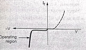
2. V‒I Characteristics of Zener Diode
•
In the forward biased condition, the normal diode and the zener diode operate
in similar fashion.
•
But zener diode is designed to operate in reverse breakdown region hence its
reverse V‒I characteristics is important.
•
When the reverse voltage is applied to zener diode, initially current is small,
which is it's reverse saturation current.
•
At a certain reverse voltage, the reverse breakdown occurs and current in the
zener diode increases rapidly. The sharp change in the zener current is called
knee or zener knee of the reverse characteristics.
•
The reverse bias voltage at which the breakdown occurs is called zener
breakdown voltage, denoted as Vz. This value is carefully designed by
controlling the doping level during manufacturing.
• The V‒I characteristics of zener diode is shown in Fig. 3.1.2.
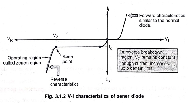
• For zener diodes, practically two currents are specified. The IZmin is minimum current through the zener diode to maintain its reverse breakdown operation.
•
The IZmax is the maximum current which zener diode can take safely
maintaining its reverse breakdown operation, i.e. constant VZ across
it. If reverse current exceeds this value, the diode may get damaged due to
excessive power dissipation.
3. Equivalent Circuit of a Zener Diode
•
Practically though very small, zener has its internal resistance.
•
In the zener region, this resistance is called dynamic resistance of the zener
denoted as ZZ.
•
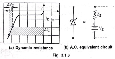
Practically zener region is not exactly vertical. The small change in zener
current Δlz produces a small change in zener voltage ΔVZ. The ratio
of ΔVZ to ΔIZ is called zener resistance ZZ.
This is shown in Fig. 3.1.3 (a).
•
Hence practically zener equivalent circuit is shown with a battery of VZ
alongwith a series resistance ZZ as indicated in Fig. 3.1.3 (b).
•
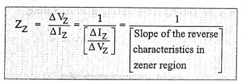
Mathematically zener resistance is given by,
ZZ
= ΔV2/ΔΙΖ
=
1 / [ΔI2/ΔVΖ]
=
1/ Slope of the reverse characteristics in zener region
4. Zener Diode Ratings
1. Zener voltage (VZ):
This is the normal working voltage of zener diode which is specified at a
specific value of zener test current IZT. The standard tolerance is ±
10 % is specified means it can vary within ±10% of its nominal value.
2. Zener test current
(IZT or IZ):
It
is the normal working current of the zener diode at which the nominal zener
voltage VZ is specified.
3. Dynamic resistance
(ZZ): It is the resistance of the zener diode
specified at normal working current and voltage but obtained as the ratio of ΔVZ
to ΔlZ.
4. Minimum zener
current (IZmin): It is minimum current
through the zener diode to maintain its reverse breakdown operation.
5. Maximum zener
current (IZmax): It is the maximum
current which zener diode can take safely without exceeding its maximum power
dissipation limit.
6. Power dissipation (PD):
It is the product of the normal zener voltage VZ and the normal
working zener current IZ.
7. Maximum power
dissipation (PD(max)): It is the maximum
power which zener diode can dissipate safely. It is the product of the normal
zener voltage VZ and the maximum zener current IZmax.
5. Comparison of Zener Diode and Conventional Diode
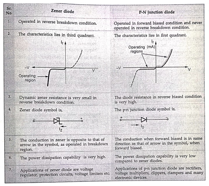
Zener
diode
1.
Operated in reverse breakdown condition.
2.
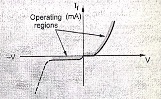
The characteristics lies in third quadrant.
3.
Dynamic zener resistance is very small in reverse breakdown condition.
4.
Zener diode symbol is, 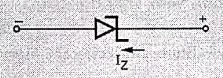
5.
The conduction in zener is opposite to that of arrow in the symbol, as operated
in breakdown region.
6.
The power dissipation capability is very high.
7.
Applications of zener diode are voltage regulator, protection circuits, voltage
limiters etc.
P‒N
junction diode
1.
Operated in forward biased condition and never operated in reverse breakdown
condition.
2.
The characteristics lies in first quadrant.
3.
The diode resistance in reverse biased condition is very high.
4.
The p‒n junction diode symbol is, 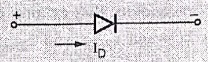
5.
The conduction when forward biased is in same direction as that of arrow in the
symbol, when forward biased.
6.
The power dissipation capability is very low compared to zener diodes.
7.
Applications of p‒n junction diode are rectifiers, voltage multipliers,
clippers, clampers and many electronic devices.
6. Applications of Zener Diode
•
The various applications of zener diode are,
1.
As a voltage regulator.
2.
In voltage clipper circuits.
3.
For controlling the output amplitude.
4.
As a reference voltage in comparator circuits.
5.
As a standard voltage source in calibrating the instruments.
Review Questions
1. Explain the breakdown mechanisms in zener diode.
2. Distinguish between zener and avalanche breakdown.
3. Draw the VI characteristics of zener diode and explain its
operation.
4. Explain the dynamic resistance and equivalent circuit of a
zener diode.
5. Explain the zener diode parameters.
6. Compare zener diode and the conventional p‒n unction diode.
7. State the applications of zener diode.
Electron Devices: Chapter 3: Special Diodes : Tag: electronics : Construction, Symbol, Breakdown Mechanisms, VI Characteristics, Equivalent Circuit Diagram, Ratings, Comparison, Applications - Zener diode
Electron Devices: Chapter 3: Special Diodes
Under Subject

Electron Devices
EC25C01 2nd Semester ECE Dept | 2025 Regulation | 2nd Semester 2025 Regulation
Related Subjects

English Essentials II
EN25C02 2nd Semester | 2025 Regulation | 2nd Semester 2025 Regulation

Tamils and Technology தமிழர்களும் தொழில்நுட்பமும்
UC25H02 2nd Semester | 2025 Regulation | 2nd Semester 2025 Regulation

Linear Algebra
MA25C02 2nd Semester | 2025 Regulation
Electron Devices
EC25C01 2nd Semester ECE Dept | 2025 Regulation | 2nd Semester 2025 Regulation

Data Structures using CPlusPlus
CS25C05 2nd Semester ECE Dept | 2025 Regulation | 2nd Semester 2025 Regulation

Circuits and Network Analysis
EC25C02 2nd Semester ECE Dept | 2025 Regulation | 2nd Semester 2025 Regulation

Re-Engineering for Innovation
ME25C05 2nd Semester | 2025 Regulation | 2nd Semester 2025 Regulation

Engineering Drawing - Laboratory
ME25C01 2nd Semester | 2025 Regulation | 2nd Semester 2025 Regulation

Data Structures using CPlusPlus - Laboratory
CS25C05 2nd Semester ECE Dept | 2025 Regulation | 2nd Semester 2025 Regulation

Devices and Circuits Laboratory
EC25C03 2nd Semester ECE Dept | 2025 Regulation | 2nd Semester 2025 Regulation