Digital Principles and Computer Organization: Chapter 12: IO Systems
IO Systems: Buses
Structure, Protocol, Clocking, Strobe Control, Handshaking
1. Bus Structure, 2. Bus Protocol, 3. Bus Clocking, 4. Synchronous Bus, 5. Asynchronous Bus, 6. Strobe Control, 7. Handshaking. Questions: 1. What is a bus? What are the different buses in a CPU? 2. Why data bus is bidirectional and address bus is unidirectional in most microprocessors ? 3. Discuss the operations of a bus. 4. What is a system bus? 5. Explain the single line bus structure. 6. Explain the multiple bus structure. 7. Draw and explain the timing diagram for synchronous input data transfer. 8. Draw and explain the timing diagram for synchronous output data transfer. 9. Explain the asynchronous data transfer using timing diagram. 10. Explain strobe controlled asynchronous data transfer. 11. Explain handshake protocol. Depict clearly how it controls data transfer during an input operation. 12. What are handshaking signals and what are the sequences of events during an input operation using handshake scheme? 13. Explain the buses.
Buses
•
The central processing unit, memory unit and I/O unit are the hardware
components/modules of the computer. They work together with communicating each
other and have paths for connecting the modules together. The collection of
paths connecting the various modules is called the interconnection structure.
•
A group of wires, called bus is used
to provide necessary signals for communication between modules.
•
A bus is a shared transmission medium
■
Must only be used by one device at a time
■
When used to connect major computer components (CPU, memory, I/O) is called a system bus.
•
The system bus is separated into three functional groups : data bus, address
bus and control bus.
• Data lines (data bus)
–
Move data between system modules
■
The data bus lines are bi–directional – CPU can read data on these lines from
memory or from a port, as well as send data out on these lines to a memory
location or to a port.
■
Width is a key factor. It determines number of bytes that can be transferred in
one cycle and hence the overall system performance.
• Address lines
(address bus) – Designate source or destination of data
on the data bus.
■
It is an unidirectional bus.
■
Width determines the maximum possible memory capacity of the system.
• Control
lines (Control bus) – Control access
to and use of the data and address lines.
1. Bus Structure
Multiple Bus Structure
• A
great number of devices on a bus will cause performance to suffer due to
■
Propagation delay – the time it takes for devices to coordinate the use of the bus.
■
The bus may become a bottleneck as the aggregate data transfer demand
approaches the capacity of the bus (in available transfer cycles / second).
• Now–a–days
the data transfer rates for video controllers and network interfaces are
growing rapidly. The need of high speed shared bus is impractical to satisfy
with a single bus. Thus, most computer systems use the multiple buses. These
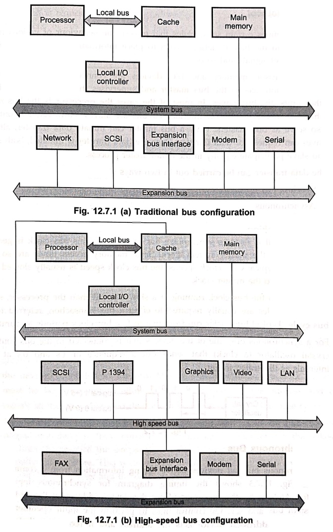
buses have the hierarchical structure as shown in Fig. 12.7.1.
Traditional hierarchical bus architecture
■
The traditional bus connection uses three buses : local bus, system bus and
expanded bus.
■
Use of a cache structure insulates CPU from frequent accesses to main memory.
■
Main memory can be moved off local bus to a system bus.
■
Expansion bus interface
o
buffers data transfers between system bus and I/O controllers on expansion bus.
o
insulates memory–to–processor traffic from I/O traffic
■
Traditional hierarchical bus breaks down as higher and higher performance is
seen in the I/O devices.
High–performance hierarchical bus architecture
■
Specifically designed to support high–capacity I/O devices.
■
It uses high–speed bus along with the three buses used in the traditional bus
connection.
■
Here, cache controller is connected to
high–speed bus.
■
This bus supports connection to high–speed LANs, such as Fiber Distributed Data
Interface (FDDI), video and graphics workstation controllers, as well as
interface controllers to local peripheral buses including SCSI and P1394.
■
Changes in processor architecture do not affect the high–speed bus and vice–versa.
2. Bus Protocol
•
Protocol defines certain set of rules that govern the behaviour of various
devices connected to the bus. It defines when to place information on the bus,
when to assert control signals and so on.
•
When processor, memory and I/O devices are connected in the system one
particular unit acts as the bus master
and supervises the use of the bus by the other units, the bus slaves. In most
of the cases the processor is the bus master, while the memory and I/O
interface circuits are slaves.
However, IO controllers also serve as bus masters. Only a bus master can
initiate data transfer, although slaves can request for data transfer. Once the
data transfer is initiated, both master and slave participate equally in the
data–transfer process.
•
The data transfer can be carried out in two ways:
■
Synchronous
■
Asynchronous
3. Bus Clocking
•
A clock signal is used to synchronize bus operations. This bus clock is
generally derived from the master system clock. Since memory access times are
so much longer than typical CPU clock speeds, the bus clock speed is usually
slowed down with respect to the master clock.
•
In addition to the bus clock running at a slower speed than the processor,
several bus clock cycles are usually required to effect a bus transaction,
referred to as a bus cycle. Typical
bus cycles run from two to five bus clock periods in duration.
•
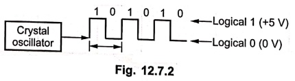
For a synchronous bus, one of the devices that is connected to the bus contains
a crystal oscillator (a clock) that sends out a sequence of 1's and 0's at
timed High intervals as illustrated in Fig. 12.7.2.
4. Synchronous Bus
•
In synchronous bus, all devices derive timing information from a common clock
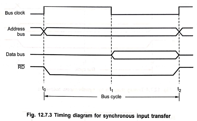
signal. Fig. 12.7.3 shows the timing diagram for synchronous input/output transfer.
At time t0, the processor places the device address on the address
lines of system bus and sets the control lines to perform the input operation.
During time t0 –t1, addressed device gets the address and
it recognizes that an input operation is
requested. At time t1, address device places its data on the data
bus. At the end of bus cycle, that, is at time t2, the processor
reads the data lines and loads the data from data bus into its input buffer.
•
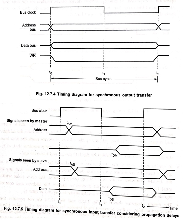
The timing diagram for an output operation is shown in Fig. 12.7.4. Here, processor
places the output data on the data lines when it transmits the address and
control line informations. At time t1, the addressed device reads
the data lines and loads the data into its data buffer. The processor simply
assumes that, at t2, the output data have been received by the I/O
device and the cycle ends.
•
In synchronous system, the clock pulse width should be chosen such that it is
greater than the maximum propagation delay between the processor and any of the
devices connected to the bus. During read operation, the clock pulse width must
be large enough to allow all devices to decode the address and control signals
so that the addressed device can be ready to respond at time t1.
• The timing diagrams shown in Fig. 12.7.3 and Fig. 12.7.4 do not consider the propagation delay so they represent ideal timings for data transfer that takes place on lines. In practice the propagation delay, delays the timings at which signals actually change state. This is illustrated in Fig. 12.7.5. Fig. 12.7.5 shows the signals as seen by the master and the other as seen by the slave.
•
The master sends address signals on the rising edge at the beginning of t0.
But due to the delay in the bus driver circuit address signals appear on the address
bus after time delay of tAM. After some more delay, at tAS,
the address signals reach the slave. The slave decodes the address and at t1
sends the requested data.
Here
again, the data signals do not appear on the data bus until tDS.
Data signals reach to the master at time tDM. At t2, the
master reads and loads the data into its input buffer. The time t2 –
tDM is known as data setup time for master's input buffer. The data
must continue to be valid after t2 for a period equal to the hold
time of the master's input buffer.
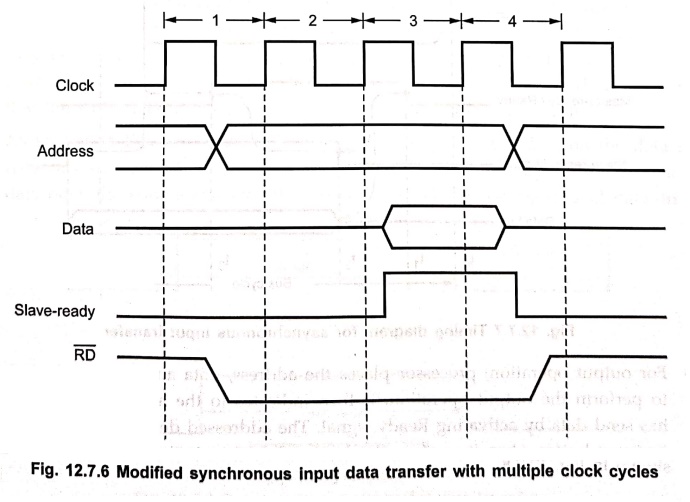
Limitations of above discussed scheme :
•
Because a transfer has to be completed within one clock cycle, the clock
period, t2–t0, must be selected to accommodate the
longest delays on the bus and the slowest device interface. This forces all
devices to operate at the speed of the slowest device.
•
There is no way determine whether the slave is responding to data transfer or
not. To overcome above mentioned limitations most of the buses includes control
signals that represent a response from the device and use high frequency clock
signal such that a complete data transfer cycle would span several clock
cycles. Then, the number of clock cycles involved can vary from one device to
another and operating speed is not decided by the slowest device. Fig. 12.7.6
shows the timing diagram for modified synchronous input data transfer with
multiple clock cycles.
5.Asynchronous Bus
•
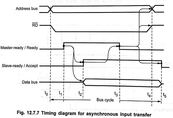
In asynchronous bus, the common clock is eliminated and data transfer on the
system bus is achieved by the use of a hand shake between the processor and the
device being addressed. Here, the clock line is replaced by two control signals
Ready and Accept.
•
For input operation, processor places the address and sets the control lines to
perform the input operation at t0. It then indicates at t1
to the addressed device that it is ready to accept data by activating the Ready
line. When the addressed device receives the Ready signal, it places the data
on the data bus at t2 and then informs the processor that it has
done so by activating the Accept line. The processor waits for accept line.
Upon activation of Accept line processor reads data from the data bus and loads
it into the input buffer the timing diagram for input operation is as shown in
Fig. 12.7.7. At t4 processor removes the address and to controls
information from bus. When the device interface receives the 1 to 0 transition
of master ready signal, it removes the data and slave–ready signal from the
bus. This completes the input data transfer.
•
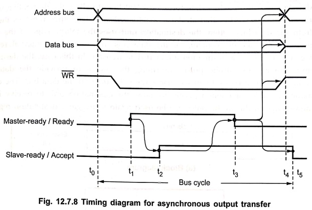
For output operation, processor places the address, data and sets the control
lines to perform the output operation. It then indicates to the addressed
device that it has send data by activating Ready signal. The addressed device
reads the data into its input buffer when it receives Ready signal. It then
indicates that it has done so by activating the Accept signal. The timing
diagram for output operation is as shown in Fig. 12.7.8.
6. Strobe Control
•
In the strobe control asynchronous data transfer, a single control line
(strobe) is used to indicate to the other unit when the transfer has to occur.
The strobe signal may be activated by either the source or the destination
unit. Fig. 12.7.9 shows a source–initiated data transfer. In this the strobe
signal informs the destination unit that the valid data is available on the
data bus from the source unit.
•
As shown in Fig. 12.7.9 (b), the source unit first places the data on the data
bus. After a data setup time (time require to settle data to steady state value
on the data bus), the source activates the strobe pulse.
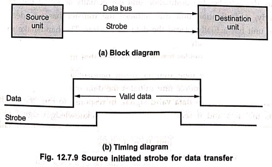
The
strobe signal and data on the data bus remain in active state for a sufficient
time to allow the destination unit to receive the data. After that strobe is
inactivated and the source removes the data from the data bus. Often, the
destination unit uses the falling edge of the strobe pulse to transfer the
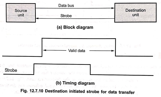
contents of the data bus into one of its internal register. Fig. 12.7.10 shows
a destination initiated data transfer. In this case, the destination unit
activates the strobe pulse, informing the source to provide the data. The
source unit in response to strobe places the valid data on the data bus. The
data is made available for enough period to allow the destination unit to
receive it. The falling edge of the strobe pulse can be used again to trigger a
destination register.
7. Handshaking
•
The disadvantage of strobe method is that the source unit that initiates the
transfer has no idea whether the destination unit has actually accepted the
data sent by it. Similarly, a destination unit that initiates the transfer has
no idea whether the source unit has actually placed the data on the bus. The handshake
method solves this problem by introducing one more signal called acknowledge signal. The acknowledge
signal provides a reply to the unit that initiates the data transfer.
•
Fig. 12.7.11 shows the data transfer using handshake signals when initiated by
source unit. Here, the source unit initiates the data transfer by placing the
data on the bus and enabling its data
valid signal. In response to
this, the destination unit accepts the data and it sends data accepted (Acknowledge) signal to the source unit. The source
unit then disables its data valid signal, which invalidates the data on the
bus. The destination unit then disables its data accepted signal and the system
goes into its initial stage.
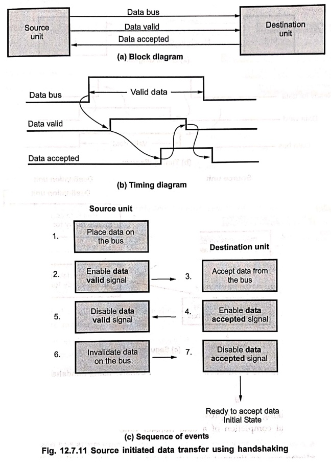
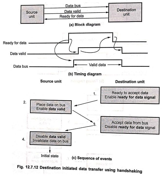
Fig.
12.7.12 shows the data transfer using handshaking signals when initiated by
destination unit. Here, the destination unit activates ready for data signal when it is ready to accept data from source
unit. In response to that, the source unit places the data on the bus and initiates
the data valid signal. The
destination unit then accepts the data from the data bus and disables the ready for data signal. Then, the source
unit disables data valid signal and invalidates data on the bus. As a result,
the system goes into its initial stage.
Advantages of handshaking scheme
1.
The handshaking scheme provides high degree of flexibility and reliability
because the successful completion of a data transfer relies on active
participation by both units.
2.
The scheme can use timeout signal to
detect any problem in the completion of data transfer. For example, if one unit
enables its handshaking control signal and if the return handshaking signal
does not respond within a given time period, the unit detects an error and
activates timeout signal to
interrupt processor. In response, processor executes a service routine that
takes appropriate error recovery action.
Review Questions
1. What is a bus? What
are the different buses in a CPU?
2. Why data bus is
bidirectional and address bus is unidirectional in most microprocessors ?
3. Discuss the
operations of a bus.
4. What is a system
bus?
5. Explain the single
line bus structure.
6. Explain the
multiple bus structure.
7. Draw and explain
the timing diagram for synchronous input data transfer.
8. Draw and explain
the timing diagram for synchronous output data transfer.
9. Explain the
asynchronous data transfer using timing diagram.
10. Explain strobe
controlled asynchronous data transfer.
11. Explain handshake
protocol. Depict clearly how it controls data transfer during an input
operation.
12. What are
handshaking signals and what are the sequences of events during an input
operation using handshake scheme?
13. Explain the buses.
Digital Principles and Computer Organization: Chapter 12: IO Systems : Tag: : Structure, Protocol, Clocking, Strobe Control, Handshaking - IO Systems: Buses
Digital Principles and Computer Organization: Chapter 12: IO Systems
Under Subject

Digital Principles and Computer Organization
CS25C06 2nd Semester AIDS, CSE, IT, CSE(CY) Dept | 2025 Regulation | 2nd Semester 2025 Regulation
Related Subjects

English Essentials II
EN25C02 2nd Semester | 2025 Regulation | 2nd Semester 2025 Regulation

Tamils and Technology தமிழர்களும் தொழில்நுட்பமும்
UC25H02 2nd Semester | 2025 Regulation | 2nd Semester 2025 Regulation

Linear Algebra
MA25C02 2nd Semester | 2025 Regulation

Applied Physics (CSIE) II
PH25C03 2nd Semester AIDS, CSE, IT, CSE(CY) Dept | 2025 Regulation | 2nd Semester 2025 Regulation
Digital Principles and Computer Organization
CS25C06 2nd Semester AIDS, CSE, IT, CSE(CY) Dept | 2025 Regulation | 2nd Semester 2025 Regulation

Basic Electrical and Electronics Engineering
EE25C01 2nd Semester | 2025 Regulation | 2nd Semester 2025 Regulation

Python for Data Science
AD25201 2nd Semester AIDS Dept | 2025 Regulation | 2nd Semester 2025 Regulation

Re-Engineering for Innovation
ME25C05 2nd Semester | 2025 Regulation | 2nd Semester 2025 Regulation

Python for Data Science - Laboratory
AD25201 2nd Semester AIDS Dept | 2025 Regulation | 2nd Semester 2025 Regulation