Digital Principles and Computer Organization: Chapter 12: IO Systems
IO Systems
Requirements, Interfacing Techniques, Memory Mapped, Types
1. Requirements of I/O System, 2. I/O Interfacing Techniques, 3. Memory Mapped I/O, I/O Mapped I/O Comparison, 4. Types of Data Transfer Techniques. Questions: 1. What is the necessity of an interface? 2. What are the functions of a typical I/O interface? 3. What are the functions performed by an I/O interface? 4. Explain the functions to be performed by a typical I/O interface with a typical input or output interface. 5. Explain how I/O devices can be interfaced with a block diagram. 6. Explain interface circuits. 7. Describe the various mechanism for accessing I/O devices. 8. Explain the following: Memory mapped I/O. 9. Give comparison between memory mapped I/O and I/O mapped I/O. 10. Compare I/O versus memory bus. 11. Distinguish between isolated and memory-mapped I/O. 12. Explain in detail about any two standard input and output interfaces required to connect the I/O device to the bus.
Digital Principles and Computer Organization:
Chapter 12: IO Systems
Introduction
•
The important components of any computer system are CPU, memory and I/O devices
(peripherals). The CPU fetches instructions (opcodes and operands/data) from
memory, processes them and stores results in memory. The other components of
the computer system (I/O devices) may be loosely called the Input/Output system.
•
The main function of I/O system is to transfer information between CPU or
memory and the outside world.
•
The important point to be noted here is, I/O devices (peripherals) cannot be
connected directly to the system bus. The reasons are discussed here.
1.
A variety of peripherals with different methods of operation are available. So
it would be impractical to incorporate the necessary logic within the CPU to
control a range of devices.
2.
The data transfer rate of peripherals is often much slower than that of the
memory or CPU. So it is impractical to use the high speed system bus to
communicate directly with the peripherals.
3.
Generally, the peripherals used in a computer system have different data
formats and word lengths than that of CPU used in it.
•
So to overcome all these difficulties, it is necessary to use a module in
between system bus and peripherals, called I/O module or I/O system, or I/O
interface.
The
functions performed by an I/O interface are :
1.
Handle data transfer between much slower peripherals and CPU or memory.
2.
Handle data transfer between CPU or memory and peripherals having different
data formats and word lengths.
3.
Match signal levels of different I/O protocols with computer signal levels.
4.
Provides necessary driving capabilities – sinking and sourcing currents.
1. Requirements of I/O System
•
The I/O system if nothing but the hardware required to connect an I/O device to
the bus. It is also called I/O
interface. The major requirements of an I/O interface are:
1.
Control and timing
2.
Processor communication
3.
Device communication
4.
Data buffering
5.
Error detection
•
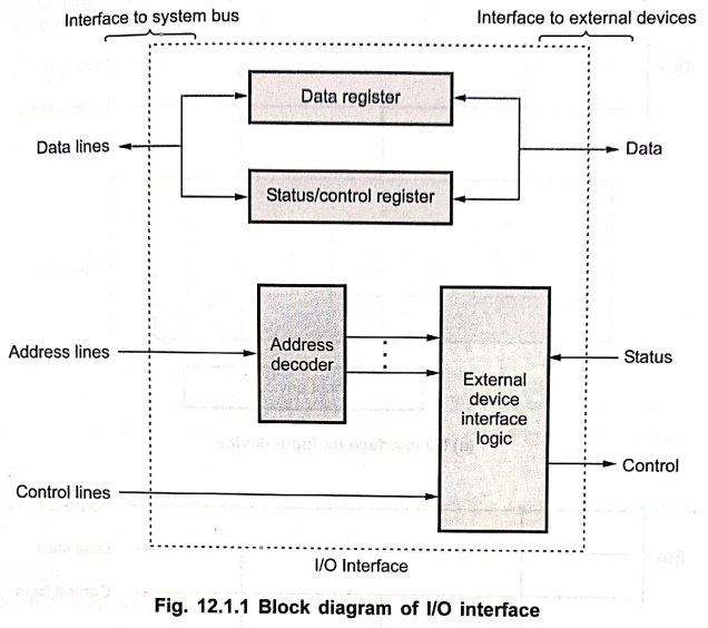
The important blocks necessary in any I/O interface are shown in Fig. 12.1.1.
•
As shown in Fig. 12.1.1, I/O interface consists of data register,
status/control register, address decoder and external device interface logic.
•
The data register holds the data being transferred to or from the processor.
•
The status/control register contains information relevant to the operation of
the I/O device. Both data and status/control registers are connected to the
data bus.
•
Address lines drive the address decoder. The address decoder enables the device
to recognize its address when address appears on the address lines.
•
The external device interface logic accepts inputs from address decoder,
processor control lines and status signal from the I/O device and generates
control signals to control the direction and speed of data transfer between
processor and I/O devices.
•
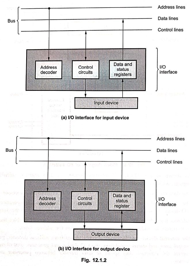
Fig. 12.1.2 shows the I/O interface for input device and output device. Here,
for simplicity block schematic of I/O interface is she instead of detail
connections.
•
The address decoder enables the device when its address appears on the address
lines.
•
The data register holds the data being transferred to or from the processor.
•
The status register contains information relevant to the operation of the I/O
device.
•
Both the data and status registers are assigned with unique addresses and they
are connected to the data bus.
2. I/O Interfacing Techniques
I/O
devices can be interfaced to a computer system I/O in two ways, which are
called interfacing techniques,
•
Memory mapped I/O
•
I/O mapped I/O
Memory mapped I/O
•
In this technique, the total memory address space is partitioned and part of
this space is devoted to I/O addressing as shown in Fig. 12.1.3.
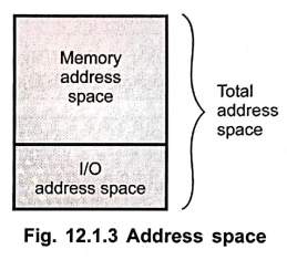
• When this technique is used, a memory reference instruction that causes data to be fetched from or stored at address specified, automatically becomes an I/O instruction if that address is made the address of an I/O port.
Advantage
•
The usual memory related instructions are used for I/O related operations. The
special I/O instructions are not required.
Disadvantage
•
The memory address space is reduced.
I/O mapped I/O
•
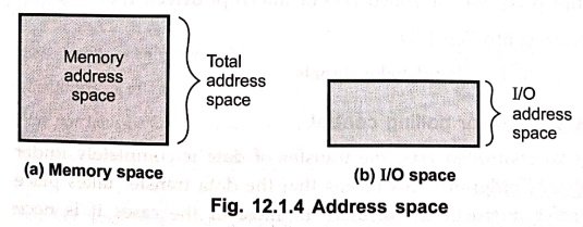
If we do not want to reduce the memory address space, we allot a different I/O
address space, apart from total memory space which is called I/O mapped I/O
technique as shown in Fig. 12.1.4.
Advantage
•
The advantage is that the full memory address space is available.
Disadvantage
•
The memory related instructions do not work. Therefore, processor can only use
this mode if it has special instructions for I/O related operations such as I/O
read, I/O write.
3. Memory Mapped I/O, I/O Mapped I/O Comparison
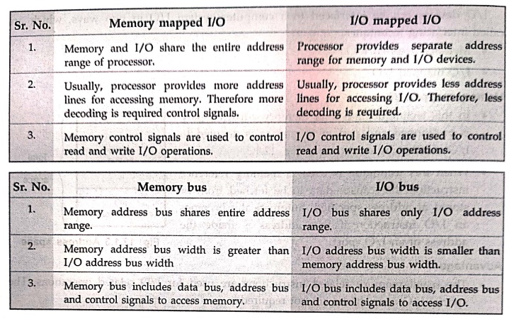
Memory mapped I/O
1.
Memory and I/O share the entire address range of processor.
2.
Usually, processor provides more address lines for accessing memory. Therefore
more decoding is required control signals.
3.
Memory control signals are used to control read and write I/O operations.
I/0 mapped I/O
1.
Processor provides separate address range for memory and I/O devices.
2.
Usually, processor provides less address lines for accessing I/O. Therefore,
less decoding is required.
3. I/O control signals are used to control read and write I/O operations.
Memory bus
1.
Memory address bus shares entire address range.
2.
Memory address bus width is greater than I/O address bus width
3.
Memory bus includes data bus, address bus and control signals to access memory.
I/O bus
1.
I/O bus shares only I/O address range.
2.
I/O address bus width is smaller than memory address bus width.
3.
I/O bus includes data bus, address bus and control signals to access I/O.
4. Types of Data Transfer Techniques
•
In I/O data transfer, the system requires the transfer of data between external
circuitry and the processor. Different ways of I/O data transfer are :
1.
Program controlled I/O or polling control.
2.
Interrupt program controlled I/O or interrupt driven I/O.
3.
Hardware controlled I/O.
4.
I/O controlled by handshake signals.
Program controlled I/O or polling control
•
In program controlled I/O, the transfer of data is completely under the control
of the processor program. This means that the data transfer takes place only
when an I/O transfer instructions executed. In most of the cases it is
necessary to check whether the device is ready for data transfer or not. To
check this, processor polls the status bit associated with the I/O device.
Interrupt program controlled I/O or interrupt driven I/O
•
In interrupt program controlled approach, when a peripheral is ready to
transfer data, it sends an interrupt signal to the processor. This indicates
that the I/O data transfer is initiated by the external I/O device.
•
When interrupted, the processor stops the execution of the program and
transfers the program control to an interrupt service routine.
•
This interrupt service routine performs the data transfer.
•
After the data transfer, it returns control to the main program at the point it
was interrupted.
Hardware controlled I/O
•
To increase the speed of data transfer between processors memory and I/O, the
hardware controlled I/O is used. It is commonly referred to as Direct Memory Access (DMA). The
hardware which controls this data transfer is commonly known as DMA controller.
•
The DMA controller sends a HOLD signal to the processor to initiate data
transfer.In response to HOLD signal, processor releases its data, address and
control buses to the DMA controller. Then the data transfer is controlled at
high speed by the DMA controller without the intervention of the processor.
•
After data transfer, DMA controller sends low on the HOLD pin, which gives the
control of data, address, and control buses back to the processor.
•
This type of data transfer is used for large data transfers.
I/O Control by handshake signals
•
The handshake signals are used to ensure the readiness of the I/O device and to
synchronize the timing of the data transfer. In this data transfer, the status
of handshaking signals are checked between the processor and an I/O device and
ort when both are ready, the actual data is transferred.
Review Questions
1. What is the
necessity of an interface?
2. What are the
functions of a typical I/O interface?
3. What are the
functions performed by an I/O interface?
4. Explain the
functions to be performed by a typical I/O interface with a typical input or
output interface.
5. Explain how I/O
devices can be interfaced with a block diagram.
6. Explain interface
circuits.
7. Describe the
various mechanism for accessing I/O devices.
8. Explain the
following : Memory mapped I/O.
9. Give comparison
between memory mapped I/O and I/O mapped I/O.
10. Compare I/O versus
memory bus.
11. Distinguish
between isolated and memory–mapped I/O.
12. Explain in detail
about any two standard input and output interfaces required to connect the I/O device
to the bus.
Digital Principles and Computer Organization: Chapter 12: IO Systems : Tag: : Requirements, Interfacing Techniques, Memory Mapped, Types - IO Systems
Digital Principles and Computer Organization: Chapter 12: IO Systems
Under Subject

Digital Principles and Computer Organization
CS25C06 2nd Semester AIDS, CSE, IT, CSE(CY) Dept | 2025 Regulation | 2nd Semester 2025 Regulation
Related Subjects

English Essentials II
EN25C02 2nd Semester | 2025 Regulation | 2nd Semester 2025 Regulation

Tamils and Technology தமிழர்களும் தொழில்நுட்பமும்
UC25H02 2nd Semester | 2025 Regulation | 2nd Semester 2025 Regulation

Linear Algebra
MA25C02 2nd Semester | 2025 Regulation

Applied Physics (CSIE) II
PH25C03 2nd Semester AIDS, CSE, IT, CSE(CY) Dept | 2025 Regulation | 2nd Semester 2025 Regulation
Digital Principles and Computer Organization
CS25C06 2nd Semester AIDS, CSE, IT, CSE(CY) Dept | 2025 Regulation | 2nd Semester 2025 Regulation

Basic Electrical and Electronics Engineering
EE25C01 2nd Semester | 2025 Regulation | 2nd Semester 2025 Regulation

Python for Data Science
AD25201 2nd Semester AIDS Dept | 2025 Regulation | 2nd Semester 2025 Regulation

Re-Engineering for Innovation
ME25C05 2nd Semester | 2025 Regulation | 2nd Semester 2025 Regulation

Python for Data Science - Laboratory
AD25201 2nd Semester AIDS Dept | 2025 Regulation | 2nd Semester 2025 Regulation