Digital Principles and Computer Organization: Chapter 2: Boolean Algebra, Logic Gates and Minimization Techniques
NAND-NAND Implementation
Question: 1. Show that if all the gates in a two-level AND-OR gate networks are replaced by NAND gates the output function does not change.
NAND–NAND
Implementation
The
implementation of a Boolean function with NAND–NAND logic requires that the
function be simplified in the sum of product form. The relationship between AND–OR
logic and NAND–NAND logic is explained using following example.
Consider
the Boolean function : Y = A B C + D
E + F.
This
Boolean function can be implemented using AND–OR logic, as shown in Fig. 2.13.1
(a).
Fig.
2.13.1 (b) shows the AND gates are replaced by NAND gates and the OR gate is
replaced by a bubbled OR gate. The implementation shown in Fig. 2.13.1 (b) is
equivalent to implementation shown in Fig. 2.13.1 (a), because two bubbled on
the same line represent double inversion (complementation) which is equivalent
to having no bubble on the line. In case of single variable, F, the
complemented variable is again complemented by bubble to produce the normal
value of F.
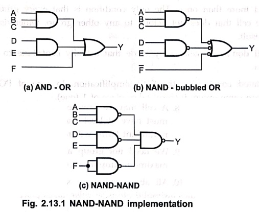
In
Fig. 2.13.1 (c), the output NAND gate is redrawn with the conventional symbol.
The NAND gate with same inputs gives complemented result, therefore  is replaced by NAND gate with F input to its both inputs. Thus all the three
implementations of Boolean function are equivalent.
is replaced by NAND gate with F input to its both inputs. Thus all the three
implementations of Boolean function are equivalent.
From
the above example we can summarize the rules for NAND–NAND logic diagram from a
Boolean function as follows :
1.
Simplify the given Boolean function and express it in sum of product form (SOP
form).
2.
Draw a NAND gate for each product term of the function that has two or more
literals. The inputs to each NAND gate are the literals of the term. This
constitutes a group of first level gates.
3.
If Boolean function includes any single literal or literals draw NAND gate for
each single literal and connect corresponding literal as an input to the NAND
gate.
4.
Draw a single NAND gate in the second level, with inputs coming from outputs of
first level gates.
Illustrative Examples
Example: 1
Implement the following
Boolean function with NAND – NAND logic
Y = AC+ ABC + ĀBC + AB +
D
Solution :
Step 1:
Simplify the given Boolean function.
Y
= AC+ ABC+ĀBC + A B+ D
= AC + BC (A + Ā ) +A B + D
= AC+ BC + A B+ D
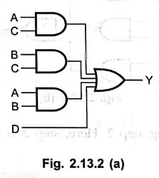
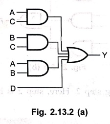
Step 2 : Implement using AND–OR logic.
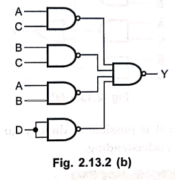
Step 3 :
Convert AND–OR logic to NAND–NAND logic.
Example: 2
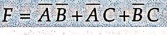
Implement the following
Boolean function with NAND–NAND logic
Solution :
Step 1 :
Implement Boolean function with AND–OR logic.
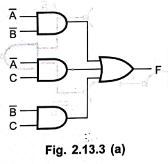
Step 2 :
Convert AND–OR NAND–NAND logic.
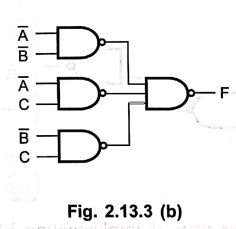
Note :
It is possible to directly go to step 2 skipping step 1. Here, step 1 is
included for clear understanding.
Example: 3
Implement the following
Boolean function with NAND–NAND logic.
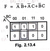
F = (A, B, C) = Σ m (0,
1, 3, 5)
Solution :
Step 1 : Simplify the given Boolean function.
Step 2 : Implement Boolean function with AND–OR logic.
Step 3 : Convert AND–OR logic to NAND–NAND logic.
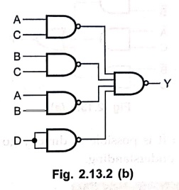
Note :
It is possible to directly go to step 3 skipping step 2. Here, step 2 is
included for clear understanding.
Examples with Solution
Example: 4
Implement EX–OR gate
using only NAND gates.
Solution :
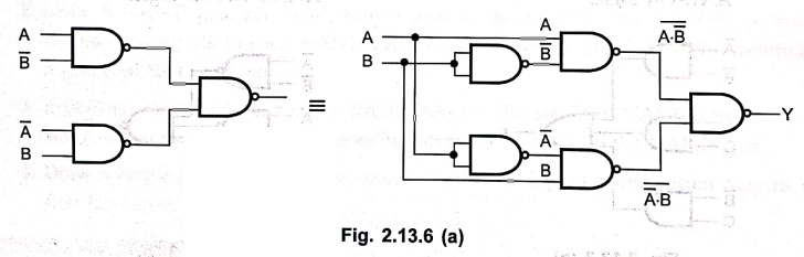
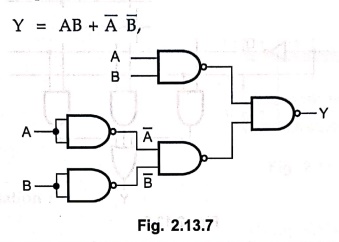
The
Boolean expression for EX–OR gate is : Y = A +
+ B. We can
implement AND–OR logic by using NAND–NAND logic as shown in Fig. 2.13.6 (b).
B. We can
implement AND–OR logic by using NAND–NAND logic as shown in Fig. 2.13.6 (b).
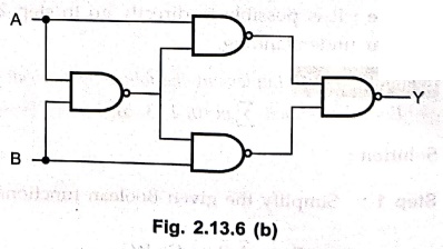
Another
way of implementing EX–OR gate using NAND gates is as shown in Fig. 2.13.6 (b).
It needs only four NAND gates.
Example: 5
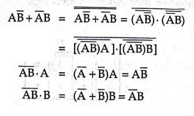
Implement EX–NOR gate
using only NAND gates.
Solution :
The
Boolean expression for EX–NOR gate is
Example: 6
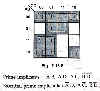
Using K–map simplify
the expression
Y(A,B,C,D) = m1+m3
+m5 +m7 +m8 +m9 +m0+m2
+m10 +m12 +m13.
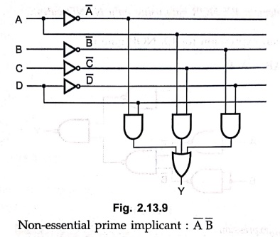
Indicate the prime
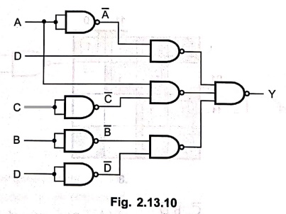
implicants, essential and non–essential prime implicants. Draw the logic
circuit using AND–OR–INVERT gates and also using NAND gates.
Solution :
Logic circuit :
Using
AND–OR–INVERT gates
Logic circuit : Using
NAND gate
We
can implement AND–OR logic by using NAND–NAND logic
Example: 7
Simplify and implement
the following POS function using NAND gates.
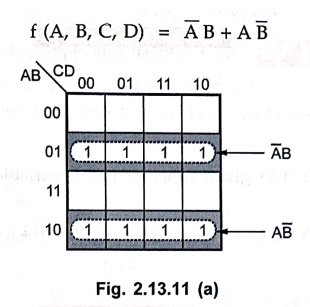
f(A, B, C, D) = II M
(0, 1, 2, 3, 12, 13, 14, 15)
Solution:
Step 1: Convert POS
function into its equivalent SOP function.
П
M (0, 1, 2, 3, 12, 13, 14, 15) = Σ m (4, 5, 6, 7, 8, 9, 10, 11)
Step 2 : K–map
simplification :
Step 3 : Implementation :
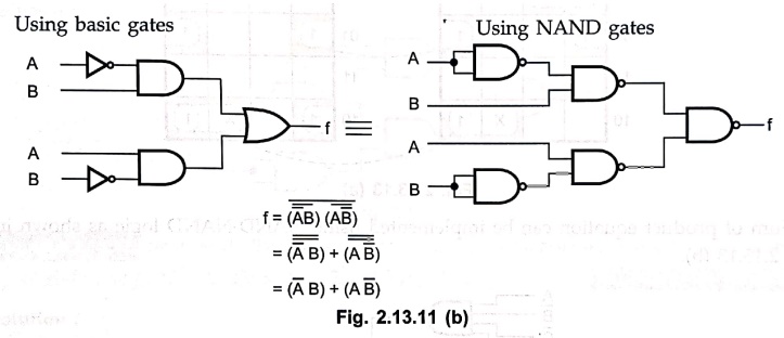
Example: 8
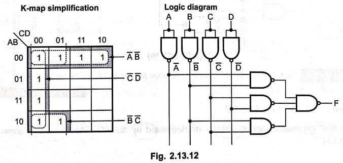
Draw a NAND logic
diagram that implements the complement of the following function.
F (A, B, C, D) = Σ (0,
1, 2, 3, 4, 8, 9, 12)
Solution :
Example: 9
Find a minimal sum–of–products
representation for
f(A,
B, C, D, E) = Σ m (1, 4, 6, 10, 20, 22, 24, 26) + d(0, 11, 16, 27) using
Karnaugh. map method. Draw the circuit of the minimal expression using only
NAND gates.
Solution :
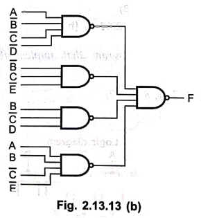
The
given function has 5 variables. Thus solving it by five variable K–map we get,
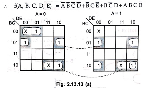
Sum
of product equation can be implemented using NAND–NAND logic as shown in Fig.
2.13.13 (b).
Example: 10
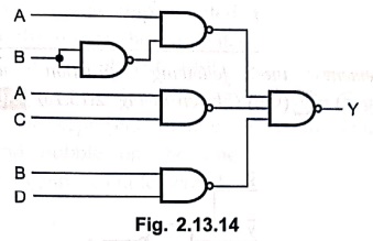
Sketch a NAND–NAND
logic circuit for the Boolean expression.
Y = AB' + AC + BD.
Solution :
Y
= A+AC+BD
The
SOP expression can be directly implemented by NAND–NAND logic as shown in Fig.
2.13.14.
Example: 11
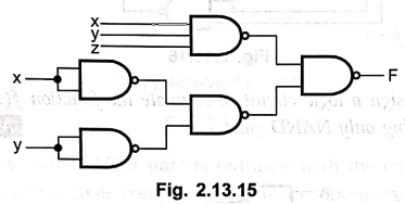
Implement using NAND
gates only, F = xyz + x'y'.
Solution :
Example: 12
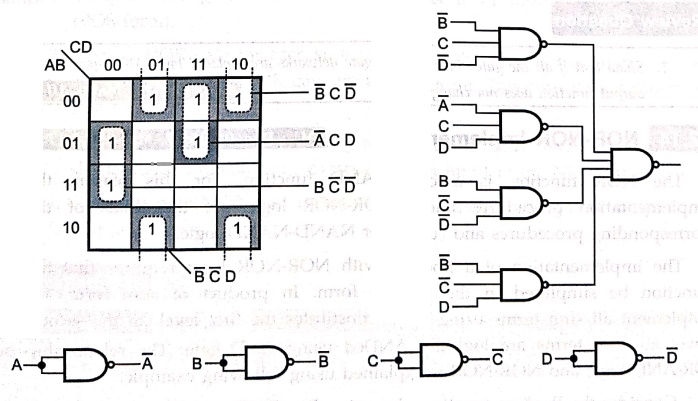
Implement the Boolean
expression using minimum number of 3 input
NAND gate ƒ(A, B, C, D)
= Σ (1,2,3,4,7,9,10,12).
Solution :
Examples for Practice
Example: 13
Implement the following
function with NAND gates.
F(x, y, z) = Σ (0,6)
(Shown in Fig. 2.13.16)
[ Answer:
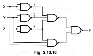
Example: 14
Design a logic circuit
to simulate the function f(A,B,C)=A(B+C)
by using only NAND gates.
[ Answer: 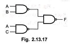 ]
]
Review Question
1. Show that if all
the gates in a two–level AND–OR gate networks are replaced by NAND gates the
output function does not change.
Digital Principles and Computer Organization: Chapter 2: Boolean Algebra, Logic Gates and Minimization Techniques : Tag: : - NAND-NAND Implementation
Digital Principles and Computer Organization: Chapter 2: Boolean Algebra, Logic Gates and Minimization Techniques
Under Subject

Digital Principles and Computer Organization
CS25C06 2nd Semester AIDS, CSE, IT, CSE(CY) Dept | 2025 Regulation | 2nd Semester 2025 Regulation
Related Subjects

English Essentials II
EN25C02 2nd Semester | 2025 Regulation | 2nd Semester 2025 Regulation

Tamils and Technology தமிழர்களும் தொழில்நுட்பமும்
UC25H02 2nd Semester | 2025 Regulation | 2nd Semester 2025 Regulation

Linear Algebra
MA25C02 2nd Semester | 2025 Regulation

Applied Physics (CSIE) II
PH25C03 2nd Semester AIDS, CSE, IT, CSE(CY) Dept | 2025 Regulation | 2nd Semester 2025 Regulation
Digital Principles and Computer Organization
CS25C06 2nd Semester AIDS, CSE, IT, CSE(CY) Dept | 2025 Regulation | 2nd Semester 2025 Regulation

Basic Electrical and Electronics Engineering
EE25C01 2nd Semester | 2025 Regulation | 2nd Semester 2025 Regulation

Python for Data Science
AD25201 2nd Semester AIDS Dept | 2025 Regulation | 2nd Semester 2025 Regulation

Re-Engineering for Innovation
ME25C05 2nd Semester | 2025 Regulation | 2nd Semester 2025 Regulation

Python for Data Science - Laboratory
AD25201 2nd Semester AIDS Dept | 2025 Regulation | 2nd Semester 2025 Regulation