Computer Organization and Architecture: Chapter 4: Memory and IO
Measuring and Improving Cache Performance
The overall goal in memory‒hierarchy design should be to achieve a performance close to that of the fastest device M1 and a cost per bit close to that of the cheapest device M.
Measuring
and Improving Cache Performance
•
The overall goal in memory‒hierarchy design should be to achieve a performance
close to that of the fastest device M1 and a cost per bit close to
that of the cheapest device Mn.
•
The performance of a memory system depends mainly on following factors.
■ Address reference
statistics : It means the order and frequency of the
logical address generated by programs that use the memory hierarchy.
■ Access time (tA)
:
The access time (tA) of each memory level relative to the CPU.
■ Storage capacity (S) :
Storage capacity of each memory level.
■ Block size :
The size of the blocks (pages) transferred between adjacent levels.
■ Allocation algorithm :
The algorithm used to determine the regions of memory to which blocks are
transferred by the block replacement process.
•
Two techniques that can be used to improve cache performance are :
■
Reducing the miss rate by reducing the probability that two different memory
blocks will contend for the same cache location.
■
Reducing the miss penalty by adding an additional level to the hierarchy. This
technique is called multilevel caching.
•
CPU time can be divided into the clock cycles that the CPU spends executing the
program and the clock cycles that the CPU spends waiting for the memory system.
CPU
time = (CPU execution clock cycles + Memory ‒ stall clock cycles) × Clock cycle
time
•
Cache hit indicates the normal CPU execution cycles.
•
Cache misses indicates the memory‒stall clock cycles.
•
Memory‒stall clock cycles are the sum of the stall cycles coming from reads
plus those coming from writes:
Memory‒stall
clock cycles = (Read‒stall cycles + Write‒stall cycles)
•
The read‒stall cycles can be defined in terms of the number of read accesses
per program, the miss penalty in clock cycles for a read and the read miss
rate:
Read‒stall
cycles = ( Reads / Program ) × Read miss rate × Read miss penalty
•
For a write‒through scheme, we have two sources of stalls : Write misses and Write buffer stalls.
• Write misses : Which
occur when we require to fetch the block before continuing the write.
• Write buffer stalls :
Which occur when the write buffer is full when a write occurs. Thus, the write
stall cycles equals the sum of these two :
Write‒stall
cycles = [ (Write / Program) × Write miss rate × Write miss penalty ] + Write
buffer stalls
•
Write‒back schemes also have potential additional stalls arising from the need
to write a cache block back to memory when the block is replaced.
•
In most write‒through cache organizations, the read and write miss penalties
are the same (the time to fetch the block from memory). If we assume that the
write buffer stalls are negligible and the read and write miss penalties are
the same, we can combine the reads and writes by using a single miss rate and
the miss penalty:
Memory‒stall
clock cycles = ( Memory accesses / Program ) × Miss rate × Miss penalty
•
We can also represent this as
Memory‒stall
clock cycles = (Instructions / Program) × (Misses / Instruction) × Miss penalty
Example: 1
Assume the miss rate of
an instruction cache is 2% and the miss rate of the data cache is 4%. If a
processor has a CPI of 2 without any memory stalls and the miss penalty is 100
cycles for all misses, determine how much faster a processor would run with a
perfect cache that never missed. Assume the frequency of all loads and stores
is 36%.
Solution :
The
number of memory miss cycles for instructors in terms of the instruction count
(I) is
Instruction
miss cycle = I × 2% × 100 = 2.00 × I
As
the frequency of all loads and stores is 36 %, we can find the number of memory
miss cycles for data references:
Data
miss cycles I × 36% × 4 % × 100 = 1.44 × I
The
total number of memory‒stall cycles is 2.00 I + 1.44 I = 3.44 I. This is move
than three cycles of memory stall per instruction. Accordingly, the total CPI
including memory stalls is 2 + 3.44 = 5.44. Since there is no change in
instruction count or clock rate, the ratio of the CPU execution times is
CPU time with stall / CPU time with perfect cache = [I × CPIstall × clock cycle] / [I × CPI perfect × clock cycle]
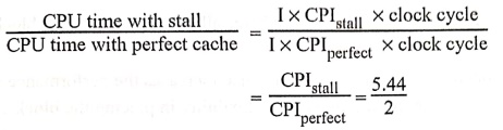
=
CPI stall / CPI perfect = 5.44 / 2
The
performance with the perfect cache is better by 5.44 / 2 = 2.72
•
Hit time is the time to access the
upper level of the memory hierarchy, which includes the time needed to
determine whether the access is a hit or miss.
•
Hit time cannot be the factor for determining the performance of the cache. The
increase in hit time means increase in the access time of the memory system
thus increasing the processor cycle time.
•
If a larger cache is used, there is increase in the access time i.e. the hit
time. But at a certain point, the increase in hit time due to larger cache
results into decrease in miss rate i.e. the hit rate increases and so the cache
performance also increases.
•
Average Memory Access Time (AMAT) is
the average time to access memory considering both hits and misses and the
frequency of different accesses.
AMAT = Time for a hit +
Miss rate × Miss penalty
•
AMAT is used as way to examine alternative cache design.
Example :
2
Calculate AMAT for a
processor with a 1 ns clock cycle time, a miss penalty of 10 clock cycles, a
miss rate of 0.05 misses per instruction and a cache access time (including hit
detection) of 1 clock cycle. Assume that the read and write miss penalties are
the same and ignore other write stalls.
Solution:
AMAT
= Time for a hit + Miss rate × Miss penalty
=
1 + 0.05 × 10
AMAT = 1.5 clock cycles
= 1.5 ns
Reducing cache misses
by more flexible placement of blocks
•
In direct mapping, the position of a memory block is given by
(Block number)
modulo (Number of blocks in the cache)
Thus,
direct mapping has one‒to‒one associativity.
•
In set‒associative mapping, there is set that contains the memory block and it
is given as (Block number) modulo (Number of sets in the cache)
•
Thus, to access a particular data all the tags of all the elements within the
particular set must be searched.
•
In a fully associative mapping as the block goes anywhere, all the tags of all
the blocks must be searched.
•
The increase in associativity decreases the miss rate and hence increases the
performance of the cache. Since fully associative mapping has maximum
flexibility in placing the blocks, it gives maximum performance.
Computer Organization and Architecture: Chapter 4: Memory and IO : Tag: Computer : - Measuring and Improving Cache Performance
Computer Organization and Architecture: Chapter 4: Memory and IO
Under Subject
Computer Organization and Architecture
CW25201 3rd Semester IT department. | 2025 Regulation | 3rd Semester 2025 Regulation
Related Subjects
Discrete Mathematics
MA25C14 3rd Semester CSE,IT,CY,AIDS departments. | 2025 Regulation | 3rd Semester 2025 Regulation
Data Structures
CS25C08 3rd Semester CSE,IT,CY,AIDS departments. | 2025 Regulation | 3rd Semester 2025 Regulation
Computer Organization and Architecture
CW25201 3rd Semester IT department. | 2025 Regulation | 3rd Semester 2025 Regulation
Object Oriented Programming
CS25C07 3rd Semester IT department. | 2025 Regulation | 3rd Semester 2025 Regulation
Web Technologies
IT25301 3rd Semester IT department. | 2025 Regulation | 3rd Semester 2025 Regulation
English Communication Skills Laboratory I
EN25C03 3rd Semester all department. | 2025 Regulation | 3rd Semester 2025 Regulation
Skill Development Course I
3rd Semester all department. | 2025 Regulation | 3rd Semester 2025 Regulation