Computer Organization and Architecture: Chapter 4: Memory and IO
Associative Memories
Questions: 1. Write a short note on associative memory. 2. Explain the role of associative memory. 3. Describe by means of block diagram how multiple matched words can be read out from an associative memory. 4. What is CAM? Explain it with block diagram. 5. Explain associative memory with its hardware organization. Explain how the data is read and write in the associative memory. 6. Attempt: Content addressable memory. 7. Give the use and role of CAM.
Associative
Memories
•
Many data‒processing applications require the search of items in a table stored
in memory. They use object names or number to identify the location of the
named or numbered object within a memory space. For example, an account number
may be searched in a file to determine the holder's name and account status. To
search an object, the number of accesses to memory depends on the location of
the object and the efficiency of the search algorithm.
•
The time required to find an object stored in memory can be reduced considerably
if objects are selected based on their contents, not on their locations. A
memory unit accessed by the content is called an associative memory or Content
Addressable Memory (CAM). This type of memory is accessed simultaneously
and in parallel on the basis of data content rather than by specific address or
location.
1. Hardware Organization
•
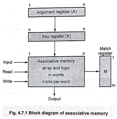
Fig. 4.7.1 shows the block diagram of an associative memory. It consists of
memory array with match logic for m n‒bit words and associated registers. The
argument register (A) and key register (K) each have n‒bits per word. Each word
in memory is compared in parallel with the contents of the argument register.
The words that match with the word stored in the argument register set a
corresponding bits in the match register. Therefore, reading can be
accomplished by a sequential access to memory for those words whose
corresponding bits in the match register have been set.
•
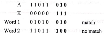
The key register provides a mask for choosing a particular field or bits in the
argument word. Only those bits in the argument register having 1's in their
corresponding position of the key register are compared. For example, if
argument register A and the key register K have the bit configuration shown
below. Only the three rightmost bits of A are compared with memory words
because K has 1's in these positions.
•
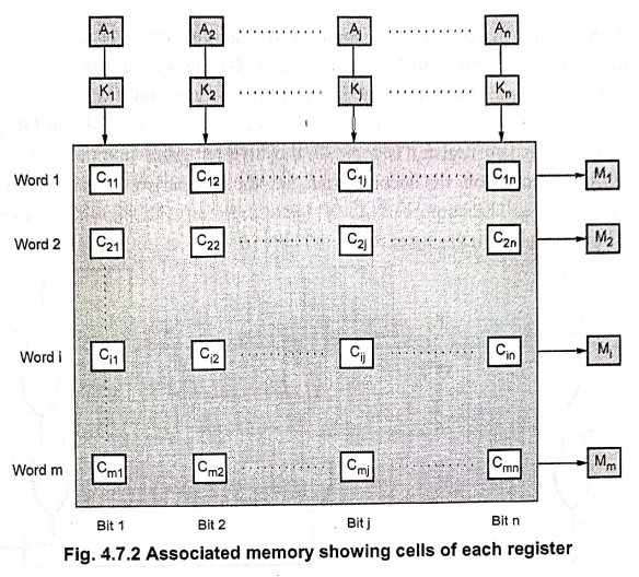
Fig. 4.7.2 shows the associated memory with cells of each register. The cells
in the memory array are marked by the letter C with two subscripts. The first
subscript gives the word number and the second subscript gives the bit position
in the word.
•
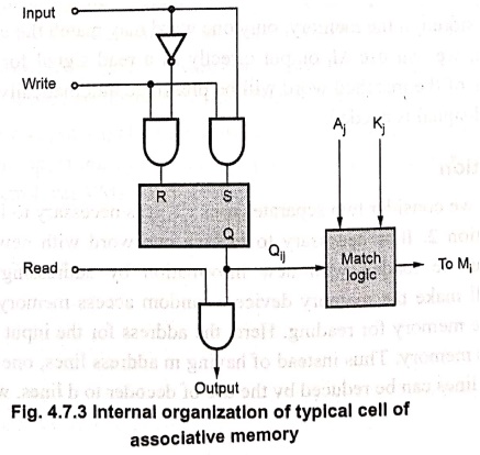
Fig. 4.7.2 shows the internal organization of a typical cell. It consists of RS
flip‒flop as a storage element and the circuit for reading, writing and
matching the cell. By making the write signal logic 1, it is possible to
transfer the input bit into the storage cell. To carry‒out read operation read
signal is made logic 1. The match logic compares the bit in the storage cell
with the corresponding unmasked bit of the argument and provides an output for
the decision logic that sets the corresponding bit in the match register.
•
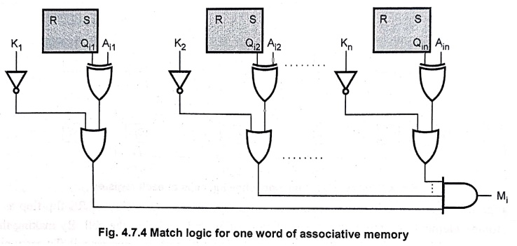
Fig. 4.7.3 shows the match logic for each word. The cell bit (Qij)
is compared with the corresponding argument bit with EX‒NOR gate. EX‒NOR gate
gives output logic 1 only when its inputs are same. The output of EX‒NOR gate
is valid only when the corresponding bit in key register is logic 1. This
condition is implemented using 2‒input OR gate. When corresponding bit in key
register is logic 1, the inverter gives output 0 which forces the output of OR
gate to follow the second input, i.e. the comparison output; otherwise output
of OR‒gate is logic 1. The outputs of all OR‒gates are then ANDed with n‒input
AND gate to check whether all bits in the word are matched with the bits in the
argument register.
2. Read Operation
•
In the read operation, all matched words are read in sequence by applying a
read signal to each word line whose corresponding Mi bit is a logic
1. In applications where no two identical items are stored in the memory, only
one word may match the unmasked argument field. In such case, we can use Mi
output directly as a read signal for the corresponding word. The contents of the
matched word will be presented automatically at the output lines and no special
read signal is needed.
3. Write Operation
•
In write operation, we consider two separate cases:
1.
It is necessary to load entire memory with new information
2.
It is necessary to replace one word with new information.
The
entire memory can be loaded with new information by addressing each location in
sequence. This will make the memory device a random access memory for writing
and a content addressable memory for reading. Here, the address for the input
can be decoded as in a random access memory. Thus instead of having m address
lines, one for each word, the number of address lines can be reduced by the use
of decoder to d lines, where m = 2d .
•
To implement the write operation in the second case the tag register is used.
This register has as many bits as there are words in the memory for every
active (valid) word stored in the memory, the corresponding bit in the tag
register is set to 1. When word is deleted from the memory the corresponding
tag bit is cleared, i.e. it is set to logic 0. The word is then stored in the
memory by scanning the tag register until the first 0 bit is encountered. This
gives the first available inactive word and a position for writing a new word.
After the new word is stored in the memory it is made active by setting the
corresponding tag bit in the tag register.
Review Questions
1. Write a short note
on associative memory.
2. Explain the role of
associative memory.
3. Describe by means
of block diagram how multiple matched words can be read out from an associative
memory.
4. What is CAM?
Explain it with block diagram.
5. Explain associative
memory with its hardware organization. Explain how the data is read and write
in the associative memory.
6. Attempt: Content
addressable memory.
7. Give the use and
role of CAM.
Computer Organization and Architecture: Chapter 4: Memory and IO : Tag: Computer : - Associative Memories
Computer Organization and Architecture: Chapter 4: Memory and IO
Under Subject
Computer Organization and Architecture
CW25201 3rd Semester IT department. | 2025 Regulation | 3rd Semester 2025 Regulation
Related Subjects
Discrete Mathematics
MA25C14 3rd Semester CSE,IT,CY,AIDS departments. | 2025 Regulation | 3rd Semester 2025 Regulation
Data Structures
CS25C08 3rd Semester CSE,IT,CY,AIDS departments. | 2025 Regulation | 3rd Semester 2025 Regulation
Computer Organization and Architecture
CW25201 3rd Semester IT department. | 2025 Regulation | 3rd Semester 2025 Regulation
Object Oriented Programming
CS25C07 3rd Semester IT department. | 2025 Regulation | 3rd Semester 2025 Regulation
Web Technologies
IT25301 3rd Semester IT department. | 2025 Regulation | 3rd Semester 2025 Regulation
English Communication Skills Laboratory I
EN25C03 3rd Semester all department. | 2025 Regulation | 3rd Semester 2025 Regulation
Skill Development Course I
3rd Semester all department. | 2025 Regulation | 3rd Semester 2025 Regulation