Computer Organization and Architecture: Chapter 4: Memory and IO
Cache Memories
Questions: 1. What is cache memory? Why is it implemented? 2. Explain the need for cache memory. 3. Explain the block diagram of cache memory system. 4. What is program locality? 5. Define locality of reference. What are its types? 6. Define the terms: spatial locality and temporal locality. 7. Explain the concept of block fetch. 8. Discuss the various mapping techniques used in cache memories. 9. What is a mapping function? What are the ways the cache can be mapped? 10. Explain about direct mapping in cache memory. 11. Explain about associative mapping in cache memory. 12. Explain about set associative mapping in cache memory. 13. Write notes on set associative mapping of cache. 14. Explain different types of mapping functions in cache memory. 15. Explain the various mapping techniques associated with cache memories. 16. Explain the various cache replacement policies in the cache memory. 17. Explain mapping functions in cache memory to determine how memory blocks are placed in cache. 18. Explain the different mapping functions that can be applied on cache memories in detail.
Cache Memories
•
In a computer system the program which is to be executed is loaded in the main
memory (DRAM). Processor then fetches the code and data from the main memory to
execute the program. The DRAMs which form the main memory are slower devices.
So it is necessary to insert wait states in memory read/write cycles. This
reduces the speed of execution.
•
To speed up the process, high speed memories such as SRAMS must be used. But
considering the cost and space required for SRAMs, it is not desirable to use
SRAMS to form the main memory. The solution for this problem is come out with
the fact that most of the microcomputer programs work with only small sections
of code and data at a particular time.
• Definition:
The part of program (code) and data that work at a particular time is usually
accessed from the SRAM memory. This is accomplished by loading the active part
of code and data from main memory to SRAM memory. This small section of SRAM
memory added between processor and main memory to speed up execution process is
known as cache memory.
•
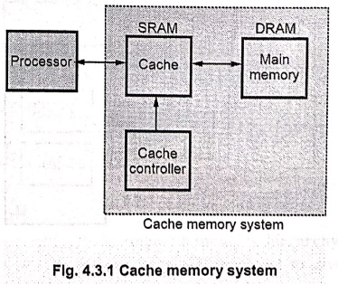
Fig. 4.3.1 shows a simplest form of cache memory system.
•
A cache memory system includes a small amount of fast memory () and a large
amount of en slow memory (DRAM). This system is configured to simulate a large
amount of fast memory.
•
Cache controller implements the cache logic. If processor finds that the
addressed code or data is not available in cache ‒ the condition referred to as
cache miss, the desired memory block
is copied from main memory to cache using cache controller. The cache
controller decides which memory block should be moved in or out of the cache
and in or out of main memory, based on the requirements. (The cache block is
also known as cache slot or cache line.)
•
The percentage of accesses where the processor finds the code or data word it
needs in the cache memory is called the hit
rate/hit ratio. The hit rate is normally greater than 90 percent.
Hit
rate = Number of hits / Total number of bus cycles × 100 %
Example: 1
The application program in a
computer system with cache uses 1400 instruction acquisition bus cycle from
cache memory and 100 from main memory. What is the hit rate? If the cache
memory operates with zero wait state and the main memory bus cycles use three
wait states, what is the average number of wait states experienced during the
program execution
Solution :
Hit
rate = 1400 / (1400 + 100) × 100 = 93.3333 %
Total
wait states = 1400 x 0 + 100 × 3 = 300
Average
wait states = Total wait states / Number of memory bus cycles = 300 /1500 = 0.2
1. Most Commonly used Cache Organizations
•
Two most commonly used system organizations for cache memory are:
■
Look‒aside and
■
Look‒through
Look ‒ aside system organization
•
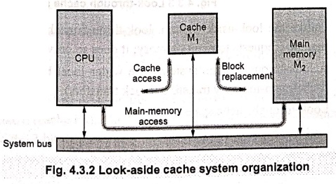
Fig. 4.3.2 shows look‒aside system of cache organization. Here, the cache and he
main memory are directly connected to the system bus.
•
In this system, the CPU initiates a memory access by placing a physical address
on the memory address bus at the start of read or write cycle.
•
The cache memory M1 immediately compares physical address to the tag
addresses currently residing in its tag memory. If a match is found, i.e., in
case of cache hit, the access is
completed by a read or write operation executed in the cache. The main memory
is not involved in the process of read or write.
•
If match is not found, i.e., in case of cache
miss, the desired access is completed by a read or write operation directed
to M2. In response to cache miss, a block of data that includes the
target address is transferred from M2 to M1. The system
bus is used for this transfer and hence it is unavailable for other uses like
I/O operations.
Look‒through system organization
•
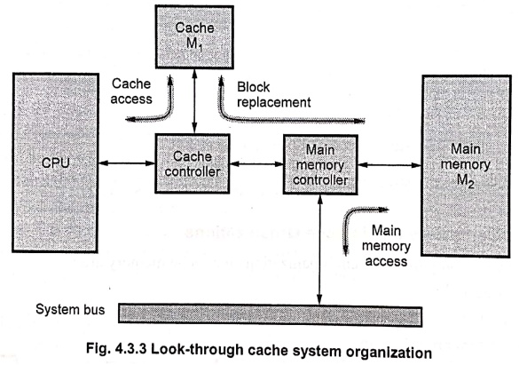
Fig. 4.3.3 shows look‒through system of cache organization. Here, the CPU
communicates with cache via a separate (local) bus which is isolated from the
main system bus. Thus during cache accesses, the system bus is available for
use by other units, such as I/O controllers, to communicate with main memory.
•
Unlike the look‒aside system, look‒through cache system does not automatically
send all memory requests to main memory; it does so only after a cache miss.
•
A look‒through cache systems use wider local bus to link M1 and M2,
thus speeding up cache‒main‒memory transfers (block transfers).
•
Look‒through cache system is faster.
Disadvantages:
■
It is complex.
■
It is costly.
■
It takes longer time for M2 to respond to the CPU when a cache miss
occurs.
Cache
read operation
•
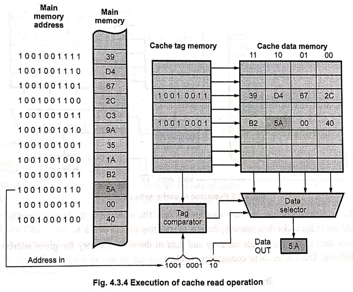
Fig. 4.3.4 shows the small cache system. Here each cache block is 4 bytes and
each memory address is 10‒bit long. Due to this 8 high‒order bits form the tag
or block address and the 2 low‒order bits define a displacement address within
the block.
•
When a block is assigned to the cache data memory, its tag is also placed in
the cache tag memory.
•
During read operation, the 8 high‒order bits of an address are compared with
stored tags in the cache tag memory to find match (cache hit). The stored tag
pinpoints the corresponding block in cache data memory and the 2‒bit
displacement is used to read the target word.
Cache write operation
•
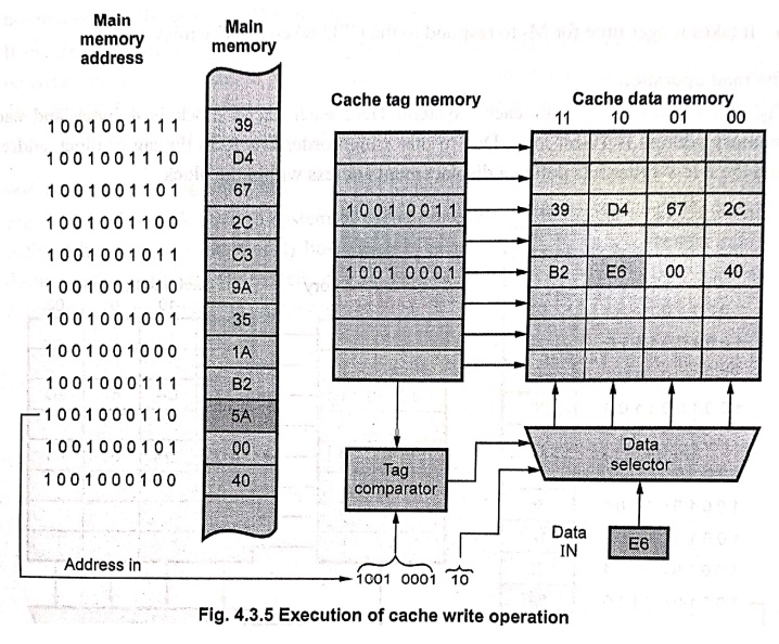
Fig. 4.3.5 shows execution of cache write operation. It uses same addressing
technique as in case of read operation.
•
When cache hit occurs, the new data, in this case E6, is stored at the location
pointed by address in the cache data memory, thereby overwriting the old data 5
A.
•
Now data in the cache data memory and data in the main memory for given address
is different. This causes cache consistency problem.
2. Program Locality
•
In cache memory system, prediction of memory location for the next access is
essential. This is possible because computer systems usually access memory from
the consecutive locations. This prediction of next memory address from the
current memory address is known as program
locality.
•
Program locality enables cache controller to get a block of memory instead of
getting just a single address.
•
The principle of program locality may not work properly when program executes
JUMP and CALL instructions. In case of these instructions, program code is not
in sequence.
3. Locality of Reference
•
We know that program may contain a simple loop, nested loops or a few
procedures that repeatedly call each other. The point is that many instructions
in localized area of the program are executed repeatedly during some time
period and the remainder of the program is accessed relatively infrequently.
This is referred to as locality of
reference.
•
It manifests itself in two ways: temporal
and spatial.
•
The temporal means that a recently
executed instruction is likely to be executed again very soon.
•
The spatial means that instructions
stored near by to the recently executed instruction are also likely to be
executed soon.
•
The temporal aspect of the locality of reference suggests that whenever an
instruction or data is first needed, it should be brought into the cache and it
should remain there until it is needed again.
•
The spatial aspect suggests that instead of bringing just one instruction or
data from the main memory to the cache, it is wise to bring several
instructions and data items that reside at adjacent address as well. We use the
term block to refer to a set of contiguous addresses of some size.
4. Block Fetch
•
Block fetch technique is used to increase the hit rate of cache.
•
A block fetch can retrieve the data located before the requested byte (look
behind) or data located after the requested byte (look ahead) or both.
•
When CPU needs to access any byte from the block, entire block that contains
the needed byte is copied from main memory into cache.
•
The size of the block is one of the most important parameters in the design of
a cache memory system.
Block size
1.
If the block size is too small, the look‒ahead and look‒behind are reduced and
therefore the hit rate is reduced.
2.
Larger blocks reduce the number of blocks that fit into a cache. As the number
of blocks decrease, block rewrites from main memory becomes more likely.
3.
Due to large size of block, the ratio of required data and useless data is
less.
4.
Bus size between the cache and the main memory increases with block size to
accommodate larger data transfers between main memory and the cache, which
increases the cost of cache memory system.
5. Elements of Cache Design
•
The cache design elements include cache size, mapping function, replacement
algorithm write policy, block size and number of caches.
Cache size :
The size of the cache should be small enough so that the overall average cost
per bit is close to that of main memory alone and large enough so that the
overall average access time is close to that of the cache alone.
Mapping function :
The cache memory can store a reasonable number of blocks at any given time, but
this number is small compared to the total number of blocks in the main memory.
Thus we have to use mapping functions to relate the main memory blocks and
cache blocks. There are two mapping functions commonly used : direct mapping
and associative mapping. Detail description of mapping functions is given in
section 4.3.6.
Replacement algorithm :
When a new block is brought into the cache, one of the existing blocks must be
replaced, by a new block.
•
There are four most common replacement algorithms:
■
Least‒Recently‒Used (LRU)
■
First‒In‒First‒Out (FIFO)
■
Least‒Frequently‒Used (LFU)
■
Random
•
Cache design change according to the choice of replacement algorithm. Detail
description of replacement algorithm is given in section 4.3.9.
Write policy :
It is also known as cache updating policy. In cache system, two copies of the
same data can exist at a time, one in cache and one in main memory. If one copy
is altered and other is not, two different sets of data become associated with
the same address. To prevent this, the cache system has updating systems such
as : write through system, buffered write through system and write‒back system.
The choice of cache write policy also change the design of cache.
Block size :
It should be optimum for cache memory system.
Number of caches :
When on‒chip cache is insufficient, the secondary cache is used. The cache
design changes as number of caches used in the system changes.
6. Mapping
•
Usually, the cache memory can store a reasonable number of memory blocks at any
given time, but this number is small compared to the total number of blocks in
the main memory. The correspondence between the main memory blocks and those in
the cache is specified by a mapping
function.
•
The mapping techniques are classified as:
1.
Direct‒mapping technique
2.
Associative‒mapping technique
■ Fully‒associative
■ Set‒associative techniques.
•
To discuss these techniques of cache mapping we consider a cache consists of
128 blocks of 16 words each, for a total of 2048 (2 K) words and assume that
the main memory has 64 K words. This 64 K words of main memory is addressable
by a 16‒bit address and it can be viewed as 4 K blocks of 16 words each. The
group of 128 blocks of 16 words each in main memory form a page.
1. Direct ‒ Mapping
•
It is the simplest mapping technique.
•
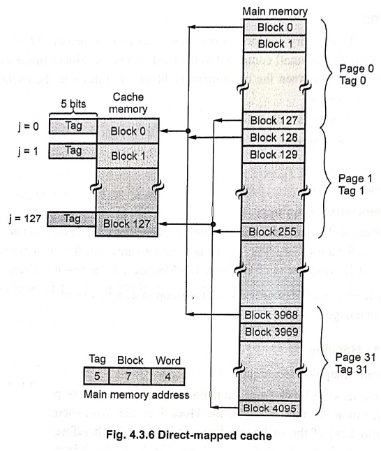
In this technique, each block from the main memory has only one possible
location in the cache organization. In this example, the block i of the main
memory maps onto block j(j = i modulo 128) of the cache, as shown in Fig. 4.3.6.
Therefore, whenever one of the main memory blocks 0, 128, 256, ...... is loaded
in the cache, it is stored in cache block 0. Blocks 1, 129, 257, ..... are
stored in cache block 1 and so on.
In
general the mapping expression is
where
j
= i modulo m
i
= Main memory block number
j
= Cache block (line) number
m
= Number of blocks (lines) in the cache
•
To implement such cache system, the address is divided into three fields, as shown in Fig. 4.3.6.
•
The lower order 4‒bits select one of the 16 words in a block. This field is
known as word field.
The second field known as block field is used to distinguish a block from other blocks. Its length is 7‒bits since 27 = 128.
•
When a new block enters the cache, the 7‒bit cache block field determines the
cache position in which this block must be stored.
•
The third field is a tag field. It
is used to store the high‒order 5‒bits of memory address of the block. These 5‒bit
(tag bits) are used to identify which of the 32 blocks (pages) that are mapped
into the cache.
•
When memory is accessed, the 7‒bit cache block field of each address generated
by CPU points to a particular block location in the cache. The high‒order 5‒bits
of the address are compared with the tag bits associated with that cache
location. If they match, then the desired word is in that block of the cache.
If there is no match, then the block containing the required word must first be
read from the main memory and loaded into the cache.
•
This means that to determine whether requested word is in the cache, only tag
field is necessary to be compared. This needs only one comparison.
•
The main drawback of direct mapped cache is that if processor needs to access
same memory locations from two different pages of the main memory frequently,
the controller has to access main memory frequently. Since only one of these
locations can be in the cache at a time. For example, if processor want to
access memory location 100 H from page 0 and then from page 2, the cache
controller has to access page 2 of the main memory. Therefore, we can say that
direct‒mapped cache is easy to implement, however, it is not very flexible.
2. Associative‒Mapping (Fully‒Associative Mapping)
•
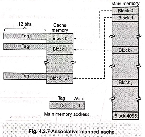
Fig. 4.3.7 associative‒mapping technique. In this technique, a main memory
block can be placed into any cache block position. As there is no fix block,
the memory address has only two fields : word
and tag. This techniques is also referred to as fully‒associative cache.
•
The 12‒tag bits are required to identify a memory block when it is resident in
the cache. The high‒order 12‒bits of an address received from the CPU are
compared to the tag bits of each block of the cache to see if the desired block
is present.
•
Once the desired block is present, the 4‒bit word is used to identify the
necessary word from the cache.
•
This technique gives complete freedom in choosing the cache location in which
to place the memory block. Thus, the memory space in the cache can be used more
efficiently.
•
A new block that has to be loaded into the cache has to replace (remove) an
existing block only if the cache is full.
•
In such situations, it is necessary to use one of the possible replacement
algorithm to select the block to be replaced.
• Disadvantage :
In associative‒mapped cache, it is necessary to compare the higher‒order bits
of address of the main memory with all 128 tag corresponding to each block to
determine whether a given block is in the cache. This is the main disadvantage
of associative‒mapped cache.
3. Set‒Associative Mapping
•
The set‒associative mapping is a of both direct and associative mapping.
•
It contains several groups of direct‒mapped blocks that operate as several
direct‒mapped caches in parallel.
•
A block of data from any page in the main memory can go into a particular block
location of any direct‒mapped cache. Hence the contention problem of the direct‒mapped
technique is eased by having a few choices for block placement.
•
The required address comparisons depend on the number of direct‒mapped caches
in the cache system. These comparisons are always less than the comparisons
required in the fully‒associative mapping.
•
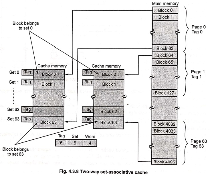
Fig. 4.3.8 shows two way set‒associative cache. Each page in the main memory is
organized in such a way that the size of each page is same as the size of one
directly mapped cache. It is called two‒way set‒associative cache because each
block from main memory has two choices for block placement.
•
In this technique, block 0, 64, 128,.....4032 of main memory can map into any
of the two (block 0) blocks of set 0, block 1, 65, 129,...., 4033 of main
memory can map into any of the two (block 1) blocks of set 1 and so on.
•
As there are two choices, it is necessary to compare address of memory with the
tag bits of corresponding two block locations of particular set. Thus for two‒way
set‒associative cache, we require two comparisons to determine whether a given
block is in the cache.
•
Since there are two direct‒mapped caches, any two bytes having same offset from
different pages can be in the cache at a time. This improves the hit rate of the cache system.
•
To implement set‒associative cache system, the address is divided into three
fields, as shown in Fig. 4.3.8.
•
The 4‒bit word field selects one of the 16 words in a block.
•
The set field needs 6‒bits to determine the desired block from 64 sets.
However, there are now 64 pages. To identify a block belongs to a particular
page from 64 pages, six tag bits are required.
Example : 2
Consider a cache consisting of 256
blocks of 16 words each, for a total of 4096 (4 K) words and assume that the
main memory is addressable by a 16‒bit address and it consists of 4 K blocks.
How many bits are there in each of the TAG, BLOCK/SET and word fields for
different mapping techniques ?
Solution :
We know that memory address is divided into three fields. We will now find the
exact bits required for each field in different mapping techniques.
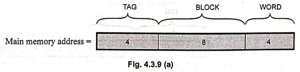
a) Direct‒mapping
Word bits: We
know that each block consists of 16 words. Therefore, to identify each word we
must have (24 = 16) four bit reserved for it.
Block bits:
The cache memory consists of 256 blocks and using direct‒mapped technique,
block k of the main memory maps onto block k modulo 256 of the cache. It has
one to one correspondence and requires unique address for each block. To
address 128 block we require (28 = 256) eight bits.
Tag bits:
The remaining 4 (16‒4‒8) address bits are tag bits which stores the higher
address of the main memory.
The
main memory address for direct‒mapping technique is divided as shown below :
b) Associative‒mapping
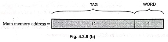
Word bits :
The word length will remain same i.e. 4 bits.
•
In the associative‒mapping technique, each block in the main memory is
identified by the tag bits and an address received from the CPU is compared
with the tag bits of each block of the cache to see if the desired block is
present. Therefore, this type of technique does not have block bits, but all
remaining bits (except word bits) are reserved as tag bits.
Block bits: 0
Tag bits:
To address each block in the main memory (212 = 4096) 12 bits are
required and therefore, there are 12 tag bits.
The
main memory address for direct mapping technique is divided as shown below :
c) Set‒associative
mapping
Let
us assume that there is a 2‒way set‒associative mapping. Here, cache memory is
mapped with two blocks per set. The set field of the address determines which
set of the cache might contain the desired block.
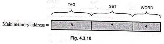
Word bits :
The word length will remain same i.e. 4 bits.
Set bits:
There are 128 sets (256/2). To identify each set (27 = 128) seven
bits are required.
Tag bits:
The remaining 5 (16‒4‒7) address bits are the tag bits which stores higher
address of the main memory.
The
main memory address for 2‒way set associative mapping technique is divided as
shown below:
Example: 3
A block set‒associative cache
consists of 64 blocks divided into 4 block sets. The main memory contains 4096
blocks, each consists of 128 words of 16 bits length:
i) How many bits are there in main
memory?
ii) How many bits are there in each
of the TAG, SET and WORD fields?
Solution :
i) Number of bits in main memory:
=
Number of blocks × Number of words per block × Number of bits per word
=
4096 × 128 × 16
=
8388608 bits
ii) Number of bits in word field:
There
are 128 words in each block. Therefore, to identify each word (27 =
128) 7 bits are required.
iii) Number of T bits in set field:
There
are 64 blocks and each set consists of 4 blocks.
Therefore,
there are 16 (64/4) sets. To identify each set (24 = 16) four bits
are required.
iv) Number of bits in tag field:
The
total words in the memory are :
4096
× 128 = 524288
To
address these words we require (219 = 524288) 19 address lines.
Therefore, tag bits are eight (19‒7‒4).
Example: 4
A digital computer has a memory
unit of 64 K × 16 and a cache memory of 1 K words. The cache uses direct
mapping with a block size of four words. How many bits there in the tag index,
block and word field of the address format ?
Solution:
Word bits:
Number of word bits = log2 4 = log2 22 = 2‒bits
Block bits:
Number of block = Cache size / Words in each block = 1K / 4 = 256
Number of block bits = log2 256 = log2 28 = 8
bits

Tag bits:
Number of bits to address main memory
=
log2 64 K = log2 216 = 16 bits
Number of Tag bits = 16‒8‒2 = 6 bits
Example: 5
A two way set associative cache
memory uses block of four words. The cache can accommodate a total of 2048
words from main memory. The main memory size is 128 K × 32.
i) How many bits are there in the
tag index, block and word field of address format?
ii) What is size of cache memory?
Solution:
Number
of bits in main memory address = log2 128 K = log 217 = 17
bits
Number
of blocks in the cache memory = 2048 /4 = 512
blocks
Number
of sets in the cache memory = 512 /2 = 256
sets
Number
of bits in set field = log2 256 = log2 28 = 8 bits
Number
of bits in word field = log2 4 = log2 22 = 2 bits
Number
of bits in tag field = 17‒8‒2 = 7 bits

Example: 6
A direct mapped cache has the
following parameters : cache size = 1 K words, Block size = 128 words and main
memory size is 64 K words. Specify the number of bits in TAG, BLOCK and WORD in
main memory address.
Solution:
Word
bits = log2 128 = 7‒bits
Number
of blocks = Cache size / Words in each block = 1 K / 128 = 8
Number
of block bits = log2 8=3‒bits
Number
of address bits to address main memory = log2 64 K = log2
216 = 16‒bits
Tag
bits = 16‒3‒7 = 6‒bits

Example : 7
How many total bits are required
for a direct‒mapped cache with 16 kB of data and 4‒word blocks, assuming a 32‒bit
address ?
Solution :
16
kB = 4K words = 212 words
Block
size of 4 words = 210 blocks
Each
block has 4 × 32 = 128 bits of data + tag + valid bit
Tag
+ valid bit = (32‒10‒2‒2) + 1= 19
Total
cache size = 210 (128 +19) = 210 × 147
Therefore,
147 kB are needed for the cache.
Example : 8
You have been asked to design a
cache with the following properties:
1) Data words are 32 bits each.
2) A cache block will contain 2048
bits of data.
3) The cache is direct mapped.
4) The address supplied from the
CPU is 32 bits long.
5) There are 2048 blocks in the
cache.
6) Addresses are to the word.
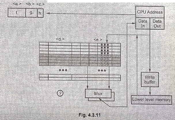
In the below Fig. 4.3.11, there are
8 fields (labeled a,b,c,d,e,f,g and h), you will need to indicate
the proper name or number of bits
for a particular portion of this cache configuration.
Solution :
f. (name)
‒ You are being asked to show what part of a physical address form the index,
offset and tag. < f > refers to the most significant bits of the address ‒so
this is the tag.
g. (name) ‒ It
follows that the next part of the address is the index.
h. (name) ‒ The
least significant bits form the offset.
c. (name)
‒ There are 211 bits / block and there are 25 bits /
word. Thus there are 26 words / block so we need 6 bits of offset.
b. (name)
‒ There are 211 blocks and the cache is direct mapped (or "1‒way
set associative"). Therefore, we need 11 bits of index.
a. (name)
‒ The remaining bits form the tag. Thus, 32‒6‒11 = 15 bits of tag.
d. (name)
‒ Field< d > refers to the fact that a tag must be stored in each block.
Thus, 15 bits are kept in each block.
e. (number)
= Field< e > asks you to specify the total number of bits / block. This
is 2048.
•
We need to compare the valid bit associated with the block, the tag stored in
the block and the tag associated with the physical address to determine if the
cache entry is useable or not. The tags should be the same and the valid bit
should be 1.
Cache size
•
There are 2048 blocks in the cache and there are 2048 bits / block. There are 8
bits / byte. Thus, there are 256 bytes/block
2048
blocks × 256 bytes / block = 219 bytes (or 0.5 MB)
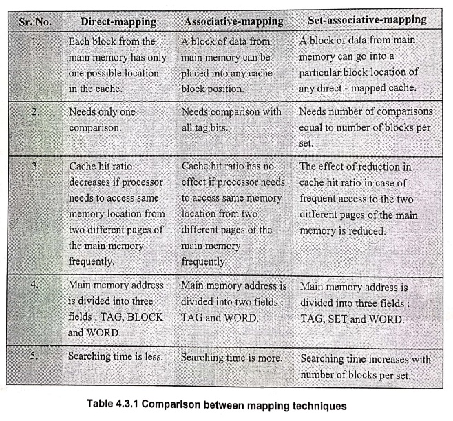
4. Comparison between Mapping Techniques
7. Cache Coherency
•
In a single CPU system, two copies of same data, one in cache memory and
another in main memory may become different. This data inconsistency is called
as cache coherence problem.
•
Cache updating systems eliminates data inconsistency in the main memory caused
by cache write operations.
•
In multiprocessor systems, another bus master can take over control of the
system bus. This bus master could write data into a main memory blocks which
are already held in the cache of another processor. When this happens, the data
in the cache no longer match those held in main memory creating inconsistency.
•
The 80386 supports four different approaches to prevent data inconsistency,
that is to protect cache coherency:
1.
Bus watching (snooping)
2.
Hardware transparency
3.
Non‒ cacheable memory
4.
Cache flushing
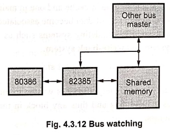
• Bus watching :
In
bus watching, cache controller invalidates the cache entry, if another master
writes to a location in shared memory which also resides in the cache memory.
Fig. 4.3.12 shows bus watching.
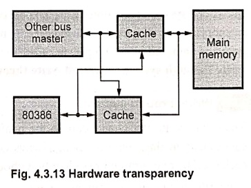
• Hardware transparency :
In
hardware transparency, accesses of all devices to the main memory are routed
through the same cache or by copying all cache writes both to the main memory
and to all other caches that share the same memory. Fig. 4.3.13 shows hardware
transparent system.
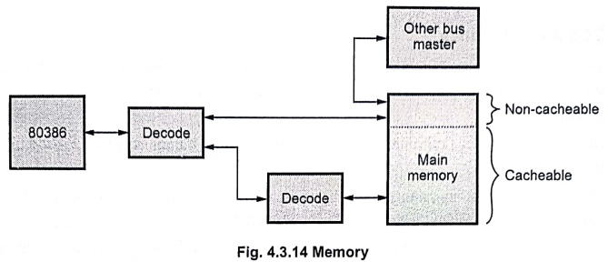
• Non‒ cacheable memory :
The
80386DX can partition its main memory into a cacheable and non‒ cacheable
memory. By designing shared memory as non‒ cacheable memory cache coherency can
be maintained, since shared memory is never copied into cache.
• Cache flushing :
To
avoid data inconsistency, a cache flush writes any altered data to the main
memory and caches in the system are flushed before a device writes to shared
memory.
8. Cache Updating Policies
•
In a cache system, two copies of same data can exist at a time, one in cache
and one in main memory. If one copy is altered and other is not, two different
sets of data become associated with the same address. To prevent this, the
cache system has updating systems such as : write through system, buffered write through system and write‒back
system.
1. Write through System
•
The cache controller copies data to the main memory immediately after it is
written to the cache. Due to this, main memory always contains a valid data and
thus any block in the cache can be overwritten immediately without data loss.
•
The write through is a simple approach.
•
This approach requires time to write
data in main memory with increase in bus traffic.
•
This in effect reduces the system
performance.
2. Buffered Write through System
•
In buffered write through system, the processor can start a new cycle before
the write cycle to the main memory is completed. This means that the write
accesses to the main memory are buffered.
•
In such systems, read access which is a "cache hit" can be performed
simultaneously when main memory is updated.
•
However, two consecutive write operations to the main memory or read operation
with cache "miss" require the processor to wait.
3. Write ‒ Back System
•
In a write‒back system, the alter
(update) bit in the tag field is used to keep information of the new data. If
it is set, the controller copies the block to main memory before loading new
data into the cache.
•
Due to one time write operation, number of write cycles are reduced in write‒back
system. But this system has following disadvantages.
■
Write‒back cache controller logic is more complex.
■
It is necessary that, all altered blocks must be written to the main memory
before another device can access these blocks in main memory.
■
In case of power failure, the data in the cache memory is lost, so there is no
way to tell which locations of the main memory contain old data. Therefore, the
main memory as well as cache must be considered volatile and provisions must be
made to save the data in the cache.
9. Replacement Algorithms
•
When a new block is brought into the cache, one of the existing blocks must be
replaced, by a new block.
•
In case of direct‒mapping cache, we know that each block from the main memory
has only one possible location in the cache, hence there is no choice. The
previous data is replaced by the data from the same memory location from new
page of the main memory.
•
For associative and set associative techniques, there is a choice of replacing
existing block. The choice of replacement of the existing block should be such
that the probability of accessing same block must be very less. The replacement
algorithms do the task of selecting the existing block which must be replaced.
•
There are four most common replacement algorithms:
■
Least‒Recently‒Used (LRU)
■
First‒In‒First‒Out (FIFO)
■
Least‒Frequently‒Used (LFU)
■
Random
• Least‒Recently‒Used :
In
this technique, the block in the set which has been in the cache longest with
no reference to it, is selected for the replacement. Since we assume that more‒
recently used memory locations are more likely to be referenced again. This
technique can be easily implemented in the two‒way set ‒ associative cache
organization.
• First‒In‒First‒Out :
This
technique uses same concept that stack implementation uses in the
microprocessors. In this technique, the block which is first loaded in the
cache amongst the present blocks in the cache is selected for the replacement.
• Least Frequently Used
:
In
this technique, the block in the set which has the fewest references is
selected for the replacement.
• Random :
Here,
there is no specific criteria for replacement of any block. The existing blocks
are replaced randomly. Simulation studies have proved that random replacement
algorithm provides only slightly inferior performance to algorithms just
discussed.
Example : 9
Consider web browsing application.
Assuming both client and server are involved in the process of web browsing
application, where can caches be placed to speed up the process? Design a
memory hierarchy for the system. Show the typical size and latency at various
levels of the hierarchy. What is the relationship between cache size and its
access latency? What are the units‒of data transfers between hierarchies? What
is the relationship between the data location, data size and transfer latency?
Solution :
a)
Assuming both client and server are involved in the process of web browsing
application, caches can be placed on both sides ‒ web browser and server.
b)
Memory hierarchy for the system is as follows:
1.
Browser cache, size = Fraction of client computer disk, Latency = Local disk latency.
2.
Proxy cache, size = Proxy disk, Latency = LAN+ Proxy disk latencies
3.
Server‒side cache, Size = Fraction of server disk,
Latency
= WAN + Server disk
4.
Server storage, size = server storage, latency = WAN + Server storage. Latency
is not directly related to cache size.
c)
The units of data transfers between hierarchies are pages.
d)
Latency grows with page size as well as distance.
Review Questions
1. What is cache
memory? Why is it implemented?
2. Explain the need
for cache memory.
3. Explain the block
diagram of cache memory system.
4. What is program
locality?
5. Define locality of
reference. What are its types?
6. Define the terms:
spatial locality and temporal locality.
7. Explain the concept
of block fetch.
8. Discuss the various
mapping techniques used in cache memories.
9. What is a mapping
function? What are the ways the cache can be mapped?
10. Explain about
direct mapping in cache memory.
11. Explain about
associative mapping in cache memory.
12. Explain about set
associative mapping in cache memory.
13. Write notes on set
associative mapping of cache.
14. Explain different
types of mapping functions in cache memory.
15. Explain the
various mapping techniques associated with cache memories.
16. Explain the
various cache replacement policies in the cache memory.
17. Explain mapping
functions in cache memory to determine how memory blocks are placed in cache.
18. Explain the
different mapping functions that can be applied on cache memories in detail.
Computer Organization and Architecture: Chapter 4: Memory and IO : Tag: Computer : - Cache Memories
Computer Organization and Architecture: Chapter 4: Memory and IO
Under Subject
Computer Organization and Architecture
CW25201 3rd Semester IT department. | 2025 Regulation | 3rd Semester 2025 Regulation
Related Subjects
Discrete Mathematics
MA25C14 3rd Semester CSE,IT,CY,AIDS departments. | 2025 Regulation | 3rd Semester 2025 Regulation
Data Structures
CS25C08 3rd Semester CSE,IT,CY,AIDS departments. | 2025 Regulation | 3rd Semester 2025 Regulation
Computer Organization and Architecture
CW25201 3rd Semester IT department. | 2025 Regulation | 3rd Semester 2025 Regulation
Object Oriented Programming
CS25C07 3rd Semester IT department. | 2025 Regulation | 3rd Semester 2025 Regulation
Web Technologies
IT25301 3rd Semester IT department. | 2025 Regulation | 3rd Semester 2025 Regulation
English Communication Skills Laboratory I
EN25C03 3rd Semester all department. | 2025 Regulation | 3rd Semester 2025 Regulation
Skill Development Course I
3rd Semester all department. | 2025 Regulation | 3rd Semester 2025 Regulation