Computer Organization and Architecture: Chapter 4: Memory and IO
Interfacing I/O Devices to the Processor, Memory and Operating System
Questions: 1. Explain the role of the operating system in handling I/O operations. Discuss why user programs cannot directly access I/O devices. 2. Describe memory‒mapped I/O and I/O‒mapped I/O. Compare both techniques. 3. What is polling ? 4. What is interrupt ? 5. What is interrupt‒driven I/O ? 6. Compare polling and interrupt‒driven I/O and explain why interrupts are preferred in most systems. 7. Write a detailed note on vectored and non‒vectored interrupts. 8. Discuss the general steps involved in interrupt driven data transfer. 9. How does the processor handle an interrupt request? 10. Why are interrupt masks provided in any processor? 11. What is a non‒maskable interrupt? What is the action performed on receipt of a NMI? 12. What are vectored interrupts ? 13. What do you mean by interrupt nesting? 14. What is priority interrupt? 15. Explain the interrupt priority schemes. 16. Explain the different types of interrupts and the different ways of handling interrupts. 17. Explain how the operating system handles interrupt priorities. Write the steps followed by the OS during interrupt handling. 18. Explain how interrupt priority levels are handled in systems like MIPS. 19. Explain the three methods of transferring data between an I/O device and memory. 20. What is DMA operation? State its advantages. 21. Why do we need DMA ? 22. Write note on : DMA. 23. Explain in detail about Direct Memory Access methods (DMA). 24. With a neat sketch explain the working principle of DMA. 25. What are the necessary operations needed to start an I/O operation using DMA ? 26. Explain how DMA transfer is accomplished with a neat diagram. 27. Explain the steps involved in the DMA operation. 28. Explain about DMA controller, with the help of a block diagram. 29. Discuss the problems caused by DMA in virtual memory and cache systems. Explain the techniques used to solve these problems.
Interfacing
I/O Devices to the Processor, Memory and Operating System
•
A bus or network protocol defines how data is sent on wires, but this is only
part of the I/O process. To move data from a device into a program's memory,
additional steps are required. This section explains how a user's I/O request
is turned into a device command, how the data is actually transferred to or
from memory and what role the operating system plays in managing and
controlling these I/O operations.
•
The operating system has a major
role in I/O because it stands between the hardware and the program that
requests I/O. The OS has these responsibilities for three reasons:
1. Many programs share
the I/O system. So the OS must manage access and avoid conflicts.
2. I/O devices use
interrupts to signal that an operation is complete or that
attention is needed. Interrupts switch the CPU to kernel mode, so only the OS can handle them.
3. Low‒level Control of
I/O devices is complicated because it requires managing
many concurrent events generated by devices and the device must be managed
carefully by following very specific rules to work correctly.
•
Because of the characteristics of I/O systems, the operating system has several
important jobs:
1.
The OS makes sure a program can use only the parts of an I/O device that it is
allowed to use. For example, it prevents a program from reading or writing a
file if it does not have permission. This protection is not possible if
programs directly access I/O devices.
2.
The OS provides easy‒to‒use routines that hide the complex, low‒level details
of device control.
3.
The OS handles interrupts from I/O devices just like it handles exceptions from
programs.
4.
The OS ensures fair access to shared I/O devices and schedules I/O operations to
improve overall system performance.
•
To do all this, the OS must communicate with I/O devices while preventing user
programs from talking to the devices directly. This communication requires
three things:
1.
The OS must be able to send commands to I/O devices, such as read, write, or
disk seek.
2.
The device must be able to inform the OS when an operation is finished or when
an error occurs.
3.
Data must be transferred between memory and the I/O device, such as moving a
block FO of data of data from a disk to memory.
1. Giving Commands to I/O Devices
•
To send a command to an I/O device, the processor must be able to address the device and send command data to it. There are two
ways to do this : memory‒mapped I/O and
special I/O instructions (I/O mapped I/O).
•
In memory‒mapped I/O, certain memory
addresses are reserved for I/O devices. When the processor reads or writes to
these addresses, the operation is treated as a command to the device not as
normal memory access.
•
When the processor writes a value to a specific I/O address, the memory system
ignores it, but the device's controller detects it, takes the data and treats
it as a command. User programs cannot do this directly because the OS does not
allow them to access the I/O address space; this protection is enforced through
address translation.
•
Memory‒mapped I/O can also be used to send or receive data. The address tells
the device what type of command it is and the data is provided by a write or
returned by a read. So, the address identifies both which device and what action
is required.
•
In real systems, performing a read or write operation usually requires many
small I/O steps, not just one. The processor may also need to check the
device's status between steps to see if the previous command finished
successfully. For example, a simple printer has two registers :
■ Status register ‒
shows whether printing is done and whether any error (like a paper jam) has
occurred.
■ Data register ‒
holds the character to be printed.
•
To print each character, the processor writes the character to the Data
register, waits until the printer sets the "done" bit in the Status
register and checks for errors. Each of these actions requires a separate I/O
access.
Comparison between Memory‒mapped I/O and I/O mapped I/O
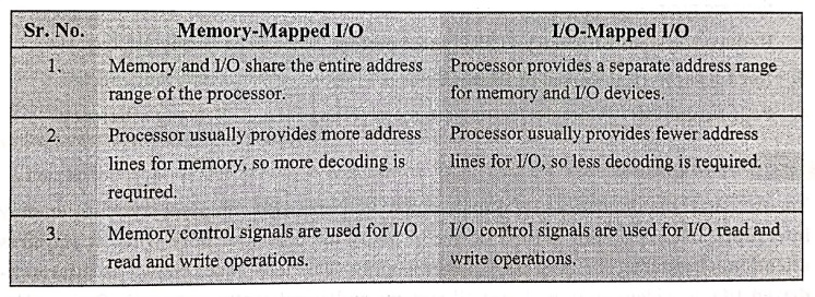
Memory‒Mapped
I/O
1.
Memory and I/O share the entire address range of the processor.
2.
Processor usually provides more address lines for memory, so more decoding is
required.
3.
Memory control signals are used for I/O read and write operations.
I/O‒Mapped I/O
1.
Processor provides a separate address range for memory and I/O devices.
2.
Processor usually provides fewer address lines for 1/0, so less decoding is
required.
3.
I/O control signals are used for I/O read and write operations.
2. Communicating with the Processor
1. Programmed I/O
•
Programmed I/O is a method in which the processor
has complete control over data transfer between an I/O device and memory.
The processor executes a fixed sequence of instructions to start, monitor and
complete each I/O operation.
•
In this technique, the processor checks
the device's status register to determine whether the device is ready. If
ready, it issues the required read or
write command and transfers data directly usually one byte or word at a
time. Multiple devices are serviced in a predefined
priority order, which can be changed by modifying the routine.
•
A key feature of Programmed I/O is polling,
where the processor repeatedly examines each device's status register to see if
it needs service. When a service request bit is set, the processor runs the corresponding
service routine. This process continues until all pending I/O requests are
handled, after which normal program execution resumes.
•
Although simple and suitable for systems with predictable I/O rates, Programmed I/O has a major drawback : it wastes processor time. Since
processors are much faster than I/O devices, continuous polling results in busy‒waiting, reducing overall system
efficiency.
Advantages
1.
Simple Implementation ‒ Easy to
design and program.
2. Complete Processor
Control ‒ Provides predictable and controlled data transfer.
3. Suitable for Real‒Time
Embedded Systems Works well when I/O rates are fixed and
timing accuracy is needed.
4. No Extra Hardware
Needed ‒ Operates entirely through software routines.
Disadvantages
1. Busy‒Waiting Wastes
CPU Time ‒ Processor repeatedly checks devices even when they
are not ready.
2. Reduced System Efficiency
‒ CPU
cannot perform other tasks during polling.
3. Not Ideal for High‒Speed
or Many Devices ‒ Processor becomes a bottleneck.
4. Poor Scalability ‒
More devices require more polling time, decreasing efficiency.
2. Interrupts
•
To overcome the limitations of programmed I/O, modern computer systems employ interrupts. Interrupts allow an I/O
device to notify the processor only when
it requires attention,
eliminating the need for constant polling. This technique, known as interrupt‒ driven I/O, is widely used in almost all systems and significantly
improves efficiency by allowing the processor to continue executing programs
until a device signals that service is needed.
•
In many situations, the computer must automatically execute a special routine
when certain events occur in the system ‒ for example, responding to input from
a keyboard, sensor, or any device that requests service. An interrupt provides
an external asynchronous signal that
informs the processor to finish its current instruction and then execute a
predefined routine called the Interrupt
Service Routine (ISR). After servicing the interrupt, the processor resumes
program execution exactly where it left off.
•
The event that triggers an interrupt is simply called an interrupt and the routine that handles it is the ISR.
Types of Interrupts
1. Hardware Interrupts
:
Hardware interrupts are generated by external devices such as keyboards,
sensors, timers and disk controllers. These interrupts occur asynchronously meaning they are not
caused by the execution of any particular instruction. They allow devices to
notify the processor when they need service, without requiring constant
polling.
2. Software Interrupts
:
Software interrupts are generated by special instructions within a program.
They are also called conditional
interrupts and are commonly used by operating systems to request system‒level
services. Unlike hardware interrupts, software
interrupts are synchronous they
occur as a direct result of program execution. They behave like exceptions,
intentionally causing the processor to transfer control to a predefined
Interrupt Service Routine (ISR).
Enabling and Disabling Interrupts
•
Most processors offer a masking
mechanism to control interrupt handling.
■
Maskable Interrupts: They can be
enabled or disabled by software. When masked, the processor ignores them even
if they occur.
■
Non‒Maskable Interrupts (NMIS) :
They cannot be disabled. Used for critical events such as hardware failures.
•
Interrupts are masked or unmasked by modifying dedicated flip‒flops or flag
bits inside the processor.
Vectored and Non‒Vectored Interrupts
•
When an external device sends an interrupt request, the processor must execute
a specific ISR. In a vectored interrupt,
the processor automatically jumps to a fixed,
predefined memory address where that ISR begins. This address is called the
vector address.
•
Because the processor directly receives the correct ISR address, vectored
interrupts provide a fast and efficient
response. Hardware immediately switches to the correct interrupt‒ handling
routine. This automated mechanism is known as interrupt vectoring. When the interrupt occurs, the processor reads
the vector address, loads it into the Program
Counter (PC) and begins executing the ISR.
•
In a non‒vectored interrupt, the
processor does not receive a specific ISR address from the device. Instead, it
always jumps to a single, fixed common
address whenever an interrupt occurs. From this common entry point,
software ‒ typically the operating system must determine which device generated the interrupt. After identifying the source,
the software branches to the correct ISR.
•
Non‒vectored interrupts are therefore slower
and less efficient, as they require more software processing before the
correct ISR can be executed.
Interrupt
Nesting
•
Some devices require immediate servicing and delaying their interrupt may cause
errors. Interrupt nesting allows a
higher‒priority interrupt to interrupt the execution of a lower‒ priority ISR.
This ensures that urgent requests are handled without delay.
Advantages of Interrupts
1. Better CPU
Utilization : CPU performs other tasks until a device
requests service.
2. Reduced Waiting Time
(No Polling) : Device notifies CPU only when service
is needed.
3. Faster System
Response : Immediate attention to urgent events.
4. Supports
Multitasking : CPU can switch quickly between tasks
and devices.
Disadvantages of Interrupts
1. More Complex
Hardware and Software: Interrupt controllers, priority
handling and ISR management add complexity.
2. Risk of Interrupt Overload : Too many interrupts can slow down the CPU.
Comparison between Programmed I/O and Interrupt‒Driven I/O
•
Table 4.10.1 gives the comparison between programmed I/O and interrupt driven
I/O.
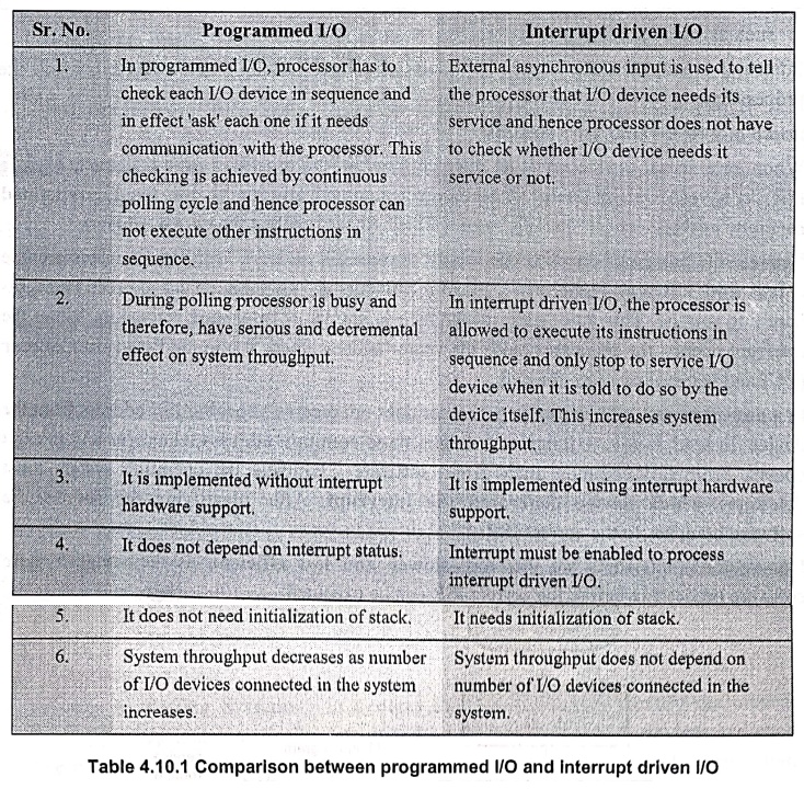
Programmed I/O
1.
In programmed I/O, processor has to check each I/O device in sequence and in
effect 'ask' each one if it needs communication with the processor. This
checking is achieved by continuous polling cycle and hence processor can not
execute other instructions in sequence.
2.
During polling processor is busy and therefore, have serious and decremental
effect on system throughput.
3.
It is implemented without interrupt hardware support.
4.
It does not depend on interrupt status.
5.
It does not need initialization of stack.
6.
System throughput decreases as number of I/O devices connected in the system
increases.
Interrupt driven I/O
1.
External asynchronous input is used to tell the processor that I/O device needs
its service and hence processor does not have to check whether I/O device needs
it service or not.
2.
In interrupt driven I/O, the processor is allowed to execute its instructions
in sequence and only stop to service I/O device when it is told to do so by the
device itself. This increases system throughput.
3.
It is implemented using interrupt hardware support.
4.
Interrupt must be enabled to process interrupt driven I/O.
5.
It needs initialization of stack.
6.
System throughput does not depend on number of I/O devices connected in the
system.
3. Recognition of Interrupt and Response to Interrupt
•
The CPU recognizes the interrupt when the external asynchronous input
(interrupt input) is asserted (a signal is sent to the interrupt input) by an
I/O device.
•
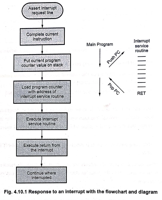
In response to an interrupt a special sequence of actions are performed. These
are as follows:
■
When a processor is interrupted, it stops executing its current program and
calls a special routine which "services" the interrupt. The event
that causes the interruption is called
interrupt and the special routine which is executed is called interrupt service routine.
1.
The processor completes its current instruction. No instruction is cut‒off in
the middle of its execution.
2.
The program counter's current contents are stored on the stack. Remember,
during the execution of an instruction the program counter is pointing to the
memory location for the next instruction.
3.
The program counter is loaded with the address of an interrupt service routine.
4.
Program execution continues with the instruction taken from the memory location
pointed by the new program counter contents.
5.
The interrupt program continues to execute until a return instruction is
executed.
6.
After execution of the RET instruction processor gets the old address (the
address of the next instruction from where the interrupt service routine was
called.) of the program counter form the stack and puts it back into the
program counter. This allows the interrupted program to continue executing at
the instruction following the one where it was interrupted. Fig. 4.10.1 shows
the response to an interrupt with the flowchart and diagram.
4. Interrupt Priority Levels
•
Different I/O devices do not have the same level of importance. Some devices
require immediate attention, while others can wait. To handle this, most
computer systems support multiple
interrupt priority levels.
•
UNIX systems, for example, typically use four
to six priority levels. These levels help the processor decide which interrupt should be serviced first
when multiple requests occur at the same time.
•
Both internal exceptions and external I/O interrupts have their own priorities.
■
Internal exceptions (such as divide‒by‒zero
or invalid instructions) generally have higher priority, because they affect
program execution directly.
■
I/O interrupts usually have lower priority, although some high‒speed
or critical I/O devices may be assigned higher priority levels.
•
Interrupt Priority can be
established using two main approaches:
1.
Software Method (Polling)
2.
Hardware Methods pro
Priority in Polling
Systems : In systems that use polling to identify the interrupting device, priority is
automatically determined by the order
in which devices are checked. The
device that is polled first naturally gets the highest priority. Therefore, no
additional hardware is needed to handle priorities.
• Hardware Methods :
■
Daisy‒Chain Priority Arrangement
■
Group‒Based Priority Arrangement
These
methods are significantly faster than software polling.
Daisy‒Chain Priority Arrangement
•
In a daisy chain, all devices share
a common Interrupt Request (INTR)
line, while the Interrupt Acknowledge
(INTA) signal passes through devices one after another in a series. This is
illustrated in Fig. 4.10.2
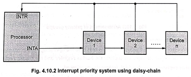
•
When multiple devices request an interrupt, they all activate the INTR line. The processor responds by
activating the INTA line. The INTA signal is first received by Device 1. If Device 1 does not need
service, it passes the signal to Device
2, and so on.
•
If Device 1 does need service, it blocks the INTA signal from going
further and places its as device
identification code on the data bus.
•
Because of this arrangement, the device
closest to the processor has the highest
priority.
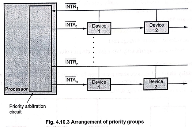
Group‒Based Priority Arrangement
•
Fig. 4.10.3 shows another method of handling interrupt priorities, which
organizes devices into groups.
■
Each group is assigned a different priority
level.
■
Within each group, devices may still be connected using a daisy‒chain arrangement.
•
In this system :
■
The processor first checks the highest‒priority
group.
■
Within that group, the device closest to the processor has priority.
■
Lower‒priority groups are checked only if no device in a higher‒priority group
requests an interrupt.
How MIPS Supports Priorities
•
MIPS processors provide hardware features that help the operating system manage
interrupt priorities. The important registers include the Status register and the Cause
register.
•
The Status register controls which
interrupts are allowed.
■
If the interrupt enable bit is 0, no interrupt is allowed.
■
The interrupt mask field allows the
OS to enable or disable specific interrupts.
•
The Cause register shows which
interrupt is pending.
•
To handle an interrupt, the operating system follows these basic steps:
1.
AND the pending interrupts with the interrupt mask to find which enabled
interrupt has occurred.
2.
Choose the highest‒priority interrupt.
3.
Save the current interrupt mask,
4.
Disable all interrupts of equal or lower
priority.
5.
Save the processor state.
6.
Enable higher‒priority interrupts.
7.
Run the correct interrupt service routine.
8.
Before restoring the state, disable interrupts so the mask field can be
restored safely.
•
An IPL (Interrupt Priority Level) is
defined by the operating system. Each process in the system is assigned an IPL.
■
At the lowest IPL, all interrupts
are allowed.
■
At the highest IPL, all interrupts
are blocked.
•
Changing the IPL simply means changing
the interrupt mask in the Status register to block or allow certain
interrupts.
3. Transferring the Data between a Device and Memory
•
We have seen two ways for a device to communicate with the processor : polling and interrupts. These two methods are also used to transfer data
between an I/O device and memory. Both work well for low‒bandwidth devices, where the focus is on keeping the device
controller simple rather than achieving high speed. In both cases, the
processor is responsible for moving the data.
1. Polling‒Based Data
Transfer : In polling, the processor repeatedly
checks the device's status and then loads data from the device's registers into
memory. This is common in real‒time systems, where timing is predictable.
2. Interrupt‒Driven
Data Transfer : Here, the processor does not constantly
check the device. Instead, the device interrupts the processor when it needs
attention.
■
The OS checks the device status.
■
If no error is found, the OS sends or receives the next byte using memory‒mapped
writes.
■
When the entire I/O request is completed, the OS informs the program.
•
This approach reduces waiting time for the processor but still requires the
processor to handle every byte
transferred. For high‒speed devices like hard disks, this overhead becomes too
large.
3. Need for a Faster Method: Direct Memory Access (DMA)
■
High‒bandwidth devices (like hard disks) transfer large blocks of data ‒
hundreds or thousands of bytes at once. Using polling or interrupts for each
byte would slow the processor significantly. To solve this, systems use Direct Memory Access (DMA).
■
DMA allows the device controller to transfer data directly between memory and
the device without involving the
processor for each byte. The interrupt system is still used, but only when
the whole transfer finishes or when an error occurs.
4. Direct Memory Access (DMA)
•
A DMA controller is a dedicated
hardware unit designed to handle high‒speed data transfers between an I/O
device and main memory without
continuous processor involvement.
•
During a DMA transfer, the DMA controller temporarily becomes the bus master, meaning it controls
communication over the system bus.
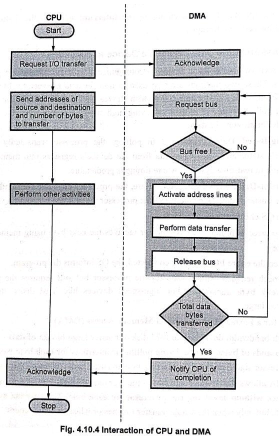
•
Fig. 4.10.4 illustrates the DMA operation by showing the interaction between
the CPU and the DMA controller. A DMA transfer consists of three main steps:
1. Processor Setup
Before
a DMA transfer begins, the processor initializes the DMA controller by
providing:
■
the I/O device involved in the
transfer
■
the direction of transfer (read from
device or write to device)
■
the starting memory address
■
the number of bytes to transfer
After
this setup, the processor can continue executing other tasks.
2. DMA Data Transfer
Once
configured, the DMA controller starts the I/O operation and proceeds with the
following steps:
a. Device Request :
When the device is ready to transfer data, it sends a DMA Request (DRQ) signal to the DMA controller.
b. Bus Request :
The DMA controller requests control of the system bus by asserting the Hold
Request (HRQ) signal to the processor.
C. Processor Response:
The processor completes its current bus operation, releases the bus and
responds with a Hold Acknowledge (HLDA)
signal.
d. DMA Gains Bus
Control : After receiving HLDA, the DMA controller takes
control of the system bus.
e. Actual Data Transfer
:
■
The DMA controller outputs the memory
address where the data will be stored.
■
It sends a DMA Acknowledge (DACK) signal
to the I/O device.
■
It asserts the I/O Read and Memory Write signals.
■
The device places the data on the data bus and the addressed memory stores it.
In this process, data moves directly
between the device and memory, without passing through the processor.
f. Address Increment :
Many DMA controllers automatically generate the next memory address and repeat
the transfer until all bytes are moved. Some also include small buffers to
smooth out timing delays.
3. DMA Completion Interrupt
When
the transfer finishes:
■
The DMA controller releases the bus (HOLD is deasserted).
■
Control returns to the processor.
■
The DMA controller sends a completion
interrupt to the processor.
■
The processor then verifies whether the transfer was successful.
•
A system may have several DMA controllers ‒ for example, one for each I/O bus.
Each one manages transfers between its own devices and main memory.
1. DMA Block Diagram
For
performing the DMA operation, the basic blocks required in a DMA
channel/controller are shown in Fig. 4.10.5.
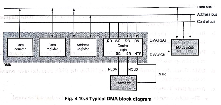
•
DMA controller communicates with the CPU via the data bus and control lines.
•
The registers in DMA are selected by the CPU through the address bus by
enabling the DS (DMA select) and RS (Register select) inputs.
•
The RD (Read) and WR (write) inputs are bidirectional.
•
When the BG (bus grant) input is 0, the CPU can communicate with the DMA
registers through the data bus to read from or write the DMA registers RD and
WR signals are input signals for DMA.
•
When BG = 1, the CPU has relinquished the buses and the DMA can communicate
directly with the memory by specifying an address in the address bus and
activating the RD or WR signals (RD and WR are now output signals for DMA). DMA
consists of data count, data register, address register and control logic.
•
Data counter register stores the number which gives the number data transfers
to be done in one DMA cycle. It is automatically decremented after each word
transfer.
•
Data register acts as buffer whereas address register initially holds the
starting address of the device. Actually, it stores the address of the next
word to be transferred. It is automatically incremented or decremented after
each word transfer.
•
After each transfer, data counter is tested for zero. When the data count
reaches zero, the DMA transfer halts.
•
The DMA controller is normally provided with an interrupts capability, in which
case it sends an interrupt to processor to signal the end of the I/O data
transfer.
2. DMA Transfer Modes
•
A DMA controller can transfer data using different modes depending on how it
accesses the system bus. The three commonly used modes are:
1. Single Transfer Mode (Cycle Stealing)
■
DMA transfers one byte/word at a time.
■
It requests the bus for each transfer and releases it immediately after.
■
Processor is paused for only one cycle.
■
Slower overall speed but minimal disturbance to the CPU.
2. Block Transfer Mode
■
DMA takes control of the bus and transfers an entire block of data continuously.
■
Processor is halted for the whole block transfer.
■
Very fast and efficient for large data transfers.
3. Demand (Burst) Transfer Mode
■
DMA transfers data as long as the device keeps requesting.
■
Bus is held until the device stops the request or the transfer completes.
■
Suitable
for fast, continuous data streams.
3. Advantages of DMA
1. High‒speed transfers
:
DMA allows high‒bandwidth I/O operations and thus suitable for large block
transfers (e.g., disk‒to‒memory).
2. Reduced processor
involvement : The CPU is active only at the start and
end of the transfer.
3. Efficient bus usage :
Data moves directly between memory and the I/O device.
5. Direct Memory Access (DMA) and the Memory System
•
When a computer uses DMA, the I/O device can transfer data directly to or from memory, without involving the processor for every piece of data.
Because of this, the normal relationship between the processor and memory changes.
•
Normally, all memory accesses. come
through the processor, which means they go through:
■
Address translation (virtual →
physical)
■
Cache (fast temporary memory)
•
But with DMA, there is a second path to
memory, which skips translation and
cache. This creates some challenges.
Problems Caused by DMA and ways to Solved Them
1. Problems with Virtual
Memory: In virtual memory, each page has :
■ a virtual address
(used by programs)
■
a physical address (used by
hardware)
DMA
must know the correct physical address to transfer data. This leads to two
issues:
■
If DMA uses virtual addresses, it
must be able to translate them, just
like the processor does.
■
If DMA uses physical addresses, then
a transfer cannot cross page boundaries
easily, because pages may not be stored next to each other in physical memory.
There
are two ways to fix this:
a. DMA uses virtual
addresses
■
The DMA controller has a small translation table.
■
The OS fills this table before starting the transfer.
b. OS splits the DMA
transfer
■
The OS breaks a large transfer into multiple small ones.
■
Each transfer fits inside one physical page.
In
both cases, the OS must make sure pages
are not moved or remapped during the DMA transfer.
2. Problems with Caches ‒ Coherence Problem :
The processor uses a cache, but DMA accesses memory directly. Because of this,
the values in cache and memory may differ.
Examples:
■
DMA writes new data to memory → cache
still has the old value
■
Processor updates data in cache only (write‒back cache) → DMA sees an old value in memory
This
is called the stale data problem or cache coherence problem.
There
are three ways to fix the cache
problem :
a. Route all I/O
through the cache
■
Ensures consistency
■
But slow and inefficient
■
Not preferred
b. Operating system
flushes or invalidates the cache
■
Before a DMA read, cache entries are removed
■
Before a DMA write, cached data is written back to memory
■
Needs some hardware support
■
Efficient and commonly used
c. Hardware‒based
selective cache invalidation
■
Hardware automatically clears or updates only the affected cache entries
■
Common in multiprocessor systems
■
Also used for I/O with DMA
Review Questions
1. Explain the role of
the operating system in handling I/O operations. Discuss why user programs
cannot directly access I/O devices.
2. Describe memory‒mapped
I/O and I/O‒mapped I/O. Compare both techniques.
3. What is polling ?
4. What is interrupt ?
5. What is interrupt‒driven
I/O ?
6. Compare polling and
interrupt‒driven I/O and explain why interrupts are preferred in most systems.
7. Write a detailed
note on vectored and non‒vectored interrupts.
8. Discuss the general
steps involved in interrupt driven data transfer.
9. How does the
processor handle an interrupt request?
10. Why are interrupt
masks provided in any processor?
11. What is a non‒maskable
interrupt? What is the action performed on receipt of a NMI?
12. What are vectored
interrupts ?
13. What do you mean
by interrupt nesting?
14. What is priority
interrupt?
15. Explain the interrupt
priority schemes.
16. Explain the
different types of interrupts and the different ways of handling interrupts.
17. Explain how the
operating system handles interrupt priorities. Write the steps followed by the
OS during interrupt handling.
18. Explain how
interrupt priority levels are handled in systems like MIPS.
19. Explain the three
methods of transferring data between an I/O device and memory.
20. What is DMA
operation? State its advantages.
21. Why do we need DMA
?
22. Write note on :
DMA.
23. Explain in detail
about Direct Memory Access methods (DMA).
24. With a neat sketch
explain the working principle of DMA.
25. What are the
necessary operations needed to start an I/O operation using DMA ?
26. Explain how DMA
transfer is accomplished with a neat diagram.
27. Explain the steps
involved in the DMA operation.
28. Explain about DMA
controller, with the help of a block diagram.
29. Discuss the
problems caused by DMA in virtual memory and cache systems. Explain the
techniques used to solve these problems.
Computer Organization and Architecture: Chapter 4: Memory and IO : Tag: Computer : - Interfacing I/O Devices to the Processor, Memory and Operating System
Computer Organization and Architecture: Chapter 4: Memory and IO
Under Subject
Computer Organization and Architecture
CW25201 3rd Semester IT department. | 2025 Regulation | 3rd Semester 2025 Regulation
Related Subjects
Discrete Mathematics
MA25C14 3rd Semester CSE,IT,CY,AIDS departments. | 2025 Regulation | 3rd Semester 2025 Regulation
Data Structures
CS25C08 3rd Semester CSE,IT,CY,AIDS departments. | 2025 Regulation | 3rd Semester 2025 Regulation
Computer Organization and Architecture
CW25201 3rd Semester IT department. | 2025 Regulation | 3rd Semester 2025 Regulation
Object Oriented Programming
CS25C07 3rd Semester IT department. | 2025 Regulation | 3rd Semester 2025 Regulation
Web Technologies
IT25301 3rd Semester IT department. | 2025 Regulation | 3rd Semester 2025 Regulation
English Communication Skills Laboratory I
EN25C03 3rd Semester all department. | 2025 Regulation | 3rd Semester 2025 Regulation
Skill Development Course I
3rd Semester all department. | 2025 Regulation | 3rd Semester 2025 Regulation