Applied Physics CSIE II: UNIT III: Nano Devices
Nano Devices: Two Marks Important Questions and Answers
Applied Physics
Anna University Part A Two Marks Important Questions and Answers - Applied Physics CSIE II: UNIT III: Nano Devices
Applied
Physics CSIE II
UNIT III:
Nano Devices
IMPORTANT PART A
QUESTIONS & ANSWERS
1. What is the
difference between the band gap of a material to the nanomaterial?
In
ordinary material, the band gap will be smaller. For nanomaterial, the band gap
will be greater.
2. In quantum dot, how
will be the nature of the material and band gap.
In
the case of quantum dots, the smaller the particle the bigger the band gap.
3. What is meant by
Ballistic transport?
When
the mean free path of the electron is longer than the dimension of the medium
through which the electron travels is called Ballistic transport.
For
Ballistic transport condition L<< Lm.
4. Define quantum
conductance.
The
quantum conductance or conductance quantum 'Go' is the quantized unit of
electrical conductance.
It
is defined as G0
= 2e2 / h = 7.748×10‒5 mho
5. Define resistance
quantum.
The
reciprocal of the conductance quantum is called resistance quantum (R0).
R0
= 1 / G0 = h / 2e2 = 12.9 kohm
6. Define quantum dot
laser.
A
quantum dot laser is a semiconductor laser that uses quantumn dots as the
active medium in its light emitting region.
7. What are the
advantages and disadvantages of quantum dot laser
Advantages:
(i)
Broad spectrum with a specific wavelength of light emission can be obtained by
changing dot size.
(ii)
Because of very small active volume, only very less population inversion is
necessary for lasing.
Disadvantages:
(i)
It is very difficult to form high quality dots [Uniform size and Higher density]
(ii)
Difficult to manufacture because of nanometer size.
8. What are the
applications of quantum dot laser?
Applications
(i)
QD lasers are used in medicine [optical coherence tomography].
(ii)
QD lasers are used in display technologies, Spectroscopy and
telecommunications. QD lasers are used in optical transmission system and
optical LANS.
9. What is meant by
bulk material?
The
bulk material is a collection of atoms having property that are from individual
atoms.
10. Define density of
energy states?
Density
of energy is defined as the number of available energy states per unit volume,
per unit energy in a solid.
11. Write the equation
for an electron density in a conductor at T = OK.
The
electron density in a conductor at T = OK is
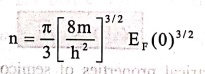
ne
= π/3 (8m/h2)3/2
. EF(0)3/2
12. Whether fermi
energy vary on material's size? If yes or no, justify your statement.
No,
since electron density is the property of the material, the Fermi energy does
not vary with materials size. Fermi energy is the same for a particle of copper
as it is for a brick of copper.
13. What will happen to
the band gap when the volume is reduced from that of a solid to a nano
material?
The
band gap gets bigger as the material gets smaller.
If
the volume is reduced from that of a solid to that of a nano material the band
gap will widen.
14. What is meant by
Tunnelling ?
The
phenomenon in which a particle, like an electron, encounters an energy barrier
in an electronic structure and suddenly penetrates is known as tunnelling.
15. What is meant by
quantum confinement?.
The
effect achieved by reducing the volume of a solid so that the energy levels
within it becomes discrete is called quantum confinement.
16. What we will
observe when we decrease the size of the particle to nano size?
It
we decrease the size of the particle to nano size, the decrease in confining
size creates the energy levels discrete. The formation of discrete energy
levels increases or widens up the band gap and finally the band gap energy also
increases.
17. What is meant by
quantum confined structure?
A
quantum confined structure is one which the motion of the electron or holes are
confined in one or more directions by potential barriers.
18. Define the term
quantum well, quantum wire and quantum dot.
An
electrically isolated region, like a thin film, where electrons are constrained
in one dimension and exhibiting quantum behaviour is called quantum well.
An
electrically isolated region, like a nano tube or nano scale wire, where
electrons constrained in two dimensions and exhibiting quantum behaviour is
called quantum wire.
An
electrically isolated region, such as a particle or a portion of a bulk semi
conductor, where electrons are constrained in all three dimensions, creating an
artificial atom that exhibits quantum behaviour is called quantum dot.
19. Write any two
applications of quantum well, quantum wire and quantum dot.
Quantum
well
1.
Quantum wells are now widely used to make semiconductor layers and other
important devices.
2.
Quantum well infrared photodetectors are also based on quantum wells, and are
used for infrared imaging.
Quantum
wire
1.
Quantum wires can be used for transistors.
2.
A quantum wire application is nano bar codes which is used in medical field.
Nano bar codes are made different quantum wires of different metals that have
different reflectivity.
Quantum
dots
1.
Quantom dot may be used as a basic building block in making a quantum computer.
2.
The quantum dot applications in various fields include blue‒laser diodes,
single electron transistor, light‒emitting devices, etc
20. How the density of
states is proportional to the energy in one dimension, two dimension and three
dimension.
(i)
In one dimension, density of states is proportional E‒1/2.
(ii)
In two dimension, density of states is proportional to energy E.
(iii)
In three dimension, density of states is proportional to E1/2.
21. Define coulomb
blockade.
The
resistance to electron transport caused by electrostatic coulomb forces in
certain electronic structures, including quantum dots and single electron
transistors is called coulomb blockade.
22. What is the purpose
of coulomb blockade?
Coulomb
blockade helps to prevent constant tunnelling to and from a quantum dot.
23. How coulomb
blockade prevent unwanted tunnelling?
The
coulomb blockade can prevent unwanted tunnelling, when energy is much higher
than the thermal energy of an electron. The condition for the coulomb blockade
is therefore Ec >> KBT
24. What is meant by
single electron transistor?
A
transistor made from a quantum dot that controls the current from source to
drain one electron at a time is called single electron transistor.
25. What are the main
criteria for the single electron phenometer to occur?
For
single electron phenomena to occur, we have to keep the single electron or
quantum dot in isolation.
26. Explain the rules
which used for the single electron phenomena to occur.
There
are two rules:
Rule
1
The
energy needed to add one electron to the dot, or charging energy, Ec, must be
significantly higher than the thermal energy of an electron
i.e.,
Ec= e2 / 2Cdot >> KBT
Rule
2
The
uncertainty of the charging energy must be less than the charging energy
itself. This is accomplished if
R1
>> h/e2
Rt
= tunnelling resistance.
By
following the above two rules, it becomes possible to manipulate electrons one
at a time and single electron phenomena will occur.
In
the single electron transistor, these two rules are used.
27. What is meant by
Carbon nano‒tubes?
Carbon
nanotubes (CNT) are molecular‒scale tubes of graphitic carbon with outstanding
properties. They are among the stiffest and strongest fibres researched till
date, with remarkable electronic properties and applications.
28. What are the types
of CNT?
Types
Carbon
nano‒tubes are of two types. viz
(i)
(a) Single walled nano‒tubes (SWNTs)
(b)
Multi walled nano‒tubes (MWNTs)
(ii)
Single walled nano‒horns (SWNHs).
29. List out of the
properties of Carbon Nano‒Tubes.
(i)
CNTs have High Electrical Conductivity.
(ii)
CNTs have Very High Tensile Strength.
(iii)
CNTs are Highly Flexible (can be bent considerably without damage).
(iv)
CNTs are Very Elastic (18% elongation to failure).
(v)
CNTs have High Thermal Conductivity.
(vi)
CNTs have a Low Thermal Expansion Coefficient.
(vii)
CNTs are Good Electron Field Emitters.
(viii)
CNTs Aspect Ratio.
30. Enumerate the
applications of CNTs in various fields.
(i)
The carbon nanotubes are very light in weight, but they are very strong, hence
they are used in aerospace.
(ii)
They are used in constructing nanoscale electronic devices.
(iii)
Carbon nano‒tubes (CNTs) are used in battery electrodes, fuel cells,
reinforcing fibers etc.
(iv)
CNTs are used in the development of flat panel displays for computer monitors
and televisions.
(v)
Plastic Composite CNTs are used as a light weight shielding materials for
protecting electromagnetic radiation.
(vi)
Light weight CNTs are also used in military and communication systems, for
protecting computers and electronic devices.
(vii)
Semiconducting CNTs are used as switching devices.
(viii)
Semiconducting CNTs are also used as chemical sensors to detect various gases.
(ix)
Nano‒tubes can also serve as catalysts for some chemical reactions.
(x)
The unique properties of carbon nanotubes will undoubtedly lead to many more
applications in future to produce nano‒computers, plastic composites etc.
Applied Physics CSIE II: UNIT III: Nano Devices : Tag: Applied Physics : Applied Physics - Nano Devices: Two Marks Important Questions and Answers
Applied Physics CSIE II: UNIT III: Nano Devices
Under Subject

Applied Physics (CSIE) II
PH25C03 2nd Semester AIDS, CSE, IT, CSE(CY) Dept | 2025 Regulation | 2nd Semester 2025 Regulation
Related Subjects

English Essentials II
EN25C02 2nd Semester | 2025 Regulation | 2nd Semester 2025 Regulation

Tamils and Technology தமிழர்களும் தொழில்நுட்பமும்
UC25H02 2nd Semester | 2025 Regulation | 2nd Semester 2025 Regulation

Linear Algebra
MA25C02 2nd Semester | 2025 Regulation
Applied Physics (CSIE) II
PH25C03 2nd Semester AIDS, CSE, IT, CSE(CY) Dept | 2025 Regulation | 2nd Semester 2025 Regulation

Digital Principles and Computer Organization
CS25C06 2nd Semester AIDS, CSE, IT, CSE(CY) Dept | 2025 Regulation | 2nd Semester 2025 Regulation

Basic Electrical and Electronics Engineering
EE25C01 2nd Semester | 2025 Regulation | 2nd Semester 2025 Regulation

Python for Data Science
AD25201 2nd Semester AIDS Dept | 2025 Regulation | 2nd Semester 2025 Regulation

Re-Engineering for Innovation
ME25C05 2nd Semester | 2025 Regulation | 2nd Semester 2025 Regulation

Python for Data Science - Laboratory
AD25201 2nd Semester AIDS Dept | 2025 Regulation | 2nd Semester 2025 Regulation