Applied Physics CSIE II: UNIT III: Nano Devices
Resonant Tunnelling Diode
Principle, Symbol, Circuit diagram, Theory, VI Characteristics, Advantages, Disadvantages, Applications

Resonant Tunnelling Diode: Principle, Symbol and Circuit diagram, Theory, Quantum Well Structure, V ‒ I Characteristics, Advantages, Disadvantages, Applications
RESONANT TUNNELLING
DIODE
Introduction
So
far we have discussed about the quantum tunnelling through a single potential
barrier. Now we are going to discuss about the quantum tunnelling through two
potential barriers (or) a potential profile.
Resonant
tunnelling occurs through a potential profile which consists of two potential
barriers, so called double barrier structure which are located very close to
each other.
Principle
Resonant
tunnelling diode works on the principle of tunnelling effect, in which the
charge carriers cross the energy barrier(s) even with lesser energy than the
barrier potential, quantum mechanically. The probability of tunnelling
increases with the decreasing barrier energy.
Symbol and Circuit diagram
The
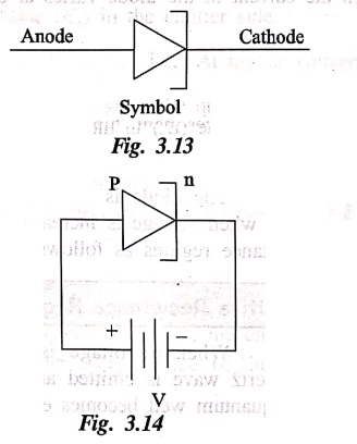
symbol and circuit diagram of a resonant tunnelling diode is as shown in Fig.
3.13 and Fig. 3.14 respectively.
Theory
A
resonant tunnelling diode also called as Essaki diode is formed using p and n‒materials,
with heavy doping say 1000 times larger than the conventional p‒n‒junction
diode. Due to heavy doping, the barrier potential decreases drastically, in
turn will help the charge carriers to easily tunnel the junctions, quantum
mechanically.
Quantum Well Structure
A
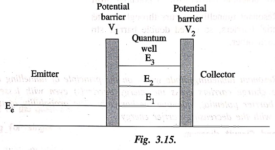
resonant tunnelling diode (RTD) consists of a quantum well structure with
discrete energy values E1, E2 etc, surrounded by two thin
layer of potential barriers (V1 and V2) with emitter (in
n‒region) and collector (in p‒region) on either side as shown in Fig. 3.15.
V ‒ I Characteristics
The
diode is forward biased as shown in Fig. 3.14. During forward bias, when
voltage is increased, then the current in the diode varies at different
resistance regions as follows.
Positive Resistance Region
When
a voltage is applied across the resonant tunnelling diode, a terahertz wave is
emitted and therefore at resonance, the energy value (E1) in the
quantum well becomes equal to the energy value (Ee) in the emitter
side.
i.e., At low voltage and at resonance ⇒ E1≈ Ee
Thus
at E1 = Ee, i.e., at resonance, the charge carriers
tunnel the potential barriers (V1 and V2) and reaches
collector region by the process called resonant
tunelling.
Therefore
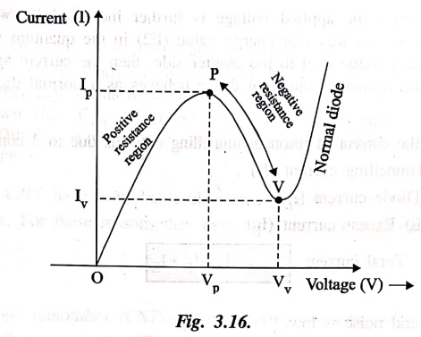
the current increases rapidly due to tunnelling effect and reaches the peak
point 'P' as shown in Fig.3.16 and this current, is called peak current (Ip).
The voltage at which the diode reaches peak current is called peak voltage (Vp).
This
region, where the current increases due to the increase in applied voltage is
called positive resistance region.
Negative Resistance Region
When
the voltage is further increased, then the terahertz wave dies out and now the
energy value (E1) in the quantum well becomes lesser than the energy
value (Ee) in the emitter side.
i.e.,
At higher voltage ⇒
E1 < Ee
However,
since the quantum well has discrete energy values, the energy value (E2)
in the quantum well is still larger than the energy value (Ee) in
the verse the emitter side as shown in Fig.3.15.
i.e., E2 > Ee
Therefore,
the charge carriers cannot tunnel the potential barriers and thus the current
in the diode decreases, and reaches the valley point 'V as shown in Fig. 3.16.
This
region where the current decreases due to increase in applied voltage is called
negative resistance region.
This
minimum current is called valley (IV) and the corresponding voltage is
called valley voltage (VV).,
Normal Diode
Now,
when the applied voltage is further increased beyond the valley point voltage
in such a way that energy value (E2) in the quantum well becomes equal to the
energy value (Ee) in the emitter side, then the current again increases and
therefore the resonant tunnelling diode behaves as a normal diode as shown in
Fig. 3.16.
Thus,
the current in resonant tunnelling diode is due to 3 components viz.,
(i)
Tunnelling current (IT)
(ii)
Diode current (ID)
and
(iii) Excess current (IE)
Total
current, ITotal = IT+ID+IE
Advantages
1.
Cost and noise is low.
2.
Fabrication is very simple.
3.
Operation speed is very high.
4.
Power dissipation is low and hence it is environmental friendly device.
Disadvantages
1.
Since it is a two terminal device, it is difficult to isolate the input and
output.
2.
It is a low output swing device.
Applications
1.
As resonant tunnelling diode has both positive resistance [From point O to P]
and negative resistance [From point P to V, it has many applications in the
switching devices,
2.
It can be used as normal diodes also.
3.
They are used as high frequency microwave oscillators.
4.
When resonant tunnelling diode is operated under negative resistance region,
then it can be used as an oscillator (or) a switch.
5.
Resonant tunnelling diode (RTD) are used in memory calls, multivalued logic
circuit devices etc.
Note:
RTD is will replace transistors as the workhorse of IC's is near future.
Applied Physics CSIE II: UNIT III: Nano Devices : Tag: Applied Physics : Principle, Symbol, Circuit diagram, Theory, VI Characteristics, Advantages, Disadvantages, Applications - Resonant Tunnelling Diode
Applied Physics CSIE II: UNIT III: Nano Devices
Under Subject

Applied Physics (CSIE) II
PH25C03 2nd Semester AIDS, CSE, IT, CSE(CY) Dept | 2025 Regulation | 2nd Semester 2025 Regulation
Related Subjects

English Essentials II
EN25C02 2nd Semester | 2025 Regulation | 2nd Semester 2025 Regulation

Tamils and Technology தமிழர்களும் தொழில்நுட்பமும்
UC25H02 2nd Semester | 2025 Regulation | 2nd Semester 2025 Regulation

Linear Algebra
MA25C02 2nd Semester | 2025 Regulation
Applied Physics (CSIE) II
PH25C03 2nd Semester AIDS, CSE, IT, CSE(CY) Dept | 2025 Regulation | 2nd Semester 2025 Regulation

Digital Principles and Computer Organization
CS25C06 2nd Semester AIDS, CSE, IT, CSE(CY) Dept | 2025 Regulation | 2nd Semester 2025 Regulation

Basic Electrical and Electronics Engineering
EE25C01 2nd Semester | 2025 Regulation | 2nd Semester 2025 Regulation

Python for Data Science
AD25201 2nd Semester AIDS Dept | 2025 Regulation | 2nd Semester 2025 Regulation

Re-Engineering for Innovation
ME25C05 2nd Semester | 2025 Regulation | 2nd Semester 2025 Regulation

Python for Data Science - Laboratory
AD25201 2nd Semester AIDS Dept | 2025 Regulation | 2nd Semester 2025 Regulation