Digital Principles and Computer Organization: Chapter 4: Combinational Circuits
Binary Adder
Half, Full Adder
Questions: 1. Design a full adder 2. Define half adder and full adder. 3. Draw a block diagram of half adder. Write truth table. Draw logic diagram. 4. Write a truth table for half adder, reduce the equation using K-map and design half adder using logic gates. 5. Define full adder. Draw logic circuit and truth table of full adder. 6. Implement full adder using two half adders.
Binary Adder
•
Digital computers perform various arithmetic operations. The most basic
operation, no doubt, is the addition of two binary digits. This simple addition
consists of four possible elementary operations, namely.
0
+ 0 = 0
0
+1 = 1
1
+ 0 = 1
1
+ 1 = 102
•
The first three operations produce a sum whose length is one digit, but when
the last operation is performed sum is two digits. The higher significant bit
of this result is called a carry,
and lower significant bit is called sum.
The logic circuit which performs this operation is called a half–adder. The circuit which performs
addition of three bits (two significant bits and a previous carry) is a full–adder.
1. Half Adder
•
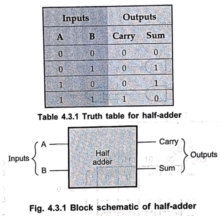
The half–adder operation needs two binary inputs : augend and addend bits; and
two binary outputs : sum and carry. The truth table shown in Table 4.3.1 gives
the relation between input and output variables for half–adder operation.
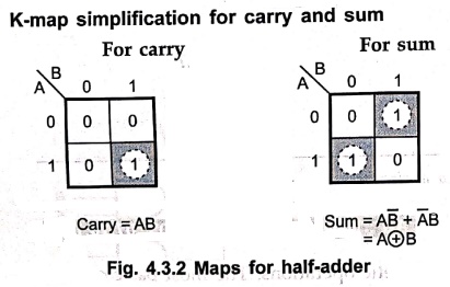
K–map simplification for carry and sum
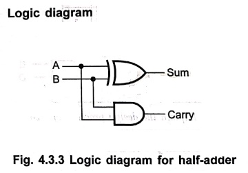
Logic diagram
Lmitation of half–adder :
•
In multidigit addition we have to add two bits along with the carry of previous
digit addition. Effectively such addition requires addition of three bits. This
is not possible with half–adder. Hence half–adders are not used in practice.
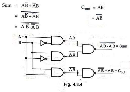
Example: 1
Draw half adder using
NAND gates.
Solution :
For
half adder :
2. Full Adder
•
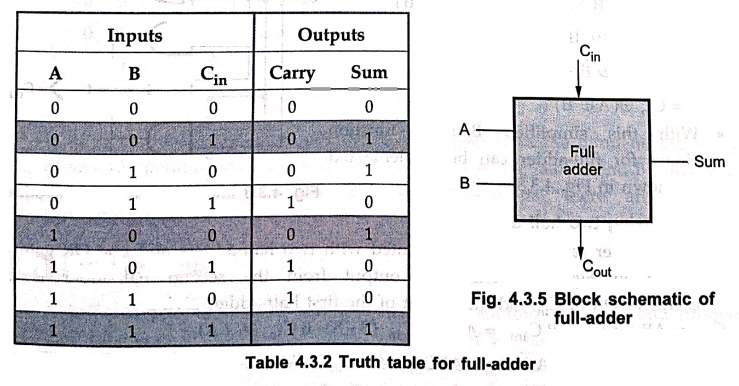
A full–adder is a combinational circuit that forms the arithmetic sum of three
input bits. It consists of three inputs and two outputs. Two of the input variables,
denoted by A and B, represent the two significant bits to be added. The third
input Cin represents the carry from the previous lower significant
position. The mue truth table for full–adder is shown in Table 4.3.2.
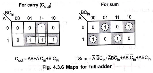
K–map simplification for carry and sum
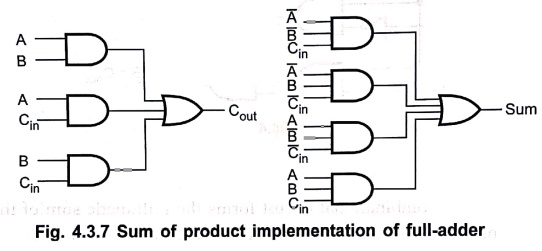
Logic diagram
•
The Boolean function for sum can be further simplified as follows :
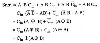
•
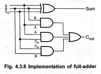
With this simplified Boolean function circuit for full–adder can be implemented
as shown in Fig. 4.3.8.
Full adder using two half adders
•
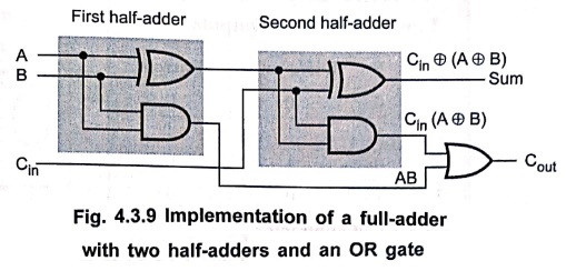
A full–adder can also be implemented with two half–adders and one OR gate, as
shown in Fig. 4.3.9. The sum output from the second half–adder is the exclusive–OR
of Cin and the output of the first half–adder, giving
Cout
= AB+ A Cin +B Cin

Review Questions
1. Design a full adder
2. Define half adder
and full adder.
3. Draw a block
diagram of half adder. Write truth table. Draw logic diagram.
4. Write a truth table
for half adder, reduce the equation using K–map and design half adder using
logic gates.
5. Define full adder.
Draw logic circuit and truth table of full adder.
6. Implement full
adder using two half adders.
Digital Principles and Computer Organization: Chapter 4: Combinational Circuits : Tag: : Half, Full Adder - Binary Adder
Digital Principles and Computer Organization: Chapter 4: Combinational Circuits
Under Subject

Digital Principles and Computer Organization
CS25C06 2nd Semester AIDS, CSE, IT, CSE(CY) Dept | 2025 Regulation | 2nd Semester 2025 Regulation
Related Subjects

English Essentials II
EN25C02 2nd Semester | 2025 Regulation | 2nd Semester 2025 Regulation

Tamils and Technology தமிழர்களும் தொழில்நுட்பமும்
UC25H02 2nd Semester | 2025 Regulation | 2nd Semester 2025 Regulation

Linear Algebra
MA25C02 2nd Semester | 2025 Regulation

Applied Physics (CSIE) II
PH25C03 2nd Semester AIDS, CSE, IT, CSE(CY) Dept | 2025 Regulation | 2nd Semester 2025 Regulation
Digital Principles and Computer Organization
CS25C06 2nd Semester AIDS, CSE, IT, CSE(CY) Dept | 2025 Regulation | 2nd Semester 2025 Regulation

Basic Electrical and Electronics Engineering
EE25C01 2nd Semester | 2025 Regulation | 2nd Semester 2025 Regulation

Python for Data Science
AD25201 2nd Semester AIDS Dept | 2025 Regulation | 2nd Semester 2025 Regulation

Re-Engineering for Innovation
ME25C05 2nd Semester | 2025 Regulation | 2nd Semester 2025 Regulation

Python for Data Science - Laboratory
AD25201 2nd Semester AIDS Dept | 2025 Regulation | 2nd Semester 2025 Regulation