Digital Principles and Computer Organization: Chapter 4: Combinational Circuits
Combinational Circuits: Two Marks Important Questions and Answers
Digital Principles and Computer Organization
Digital Principles and Computer Organization: Chapter 4: Combinational Circuits: Anna University Part A Two Marks Important Questions and Answers
Digital Principles and Computer Organization:
Chapter 4: Combinational Circuits
Two Marks Questions
with Answers
1. Define
a combinational logic circuit. Give an example.
Answer: When logic gates are
connected together to produce a specified output for certain specified
combinations of input variables, with no storage involved, the resulting
circuit is called 'combinational logic circuit'.
A
combinational circuit consists of input variables, logic gates and output
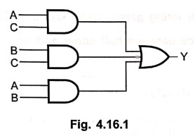
variables. For example, consider following Boolean expression,
Y
= AB + BC + AC
The
combinational logic circuit for this would require 3 AND gates and 1 OR gate as
follows :
2.
Enumerate some of the combinational circuits.
Answer: Combinational circuits are :
•
Adders
•
Subtractors
•
Multiplexers
•
Demultiplexers
•
Encoders
•
Decoders.
3. Explain
the design procedure for combinational circuits.
The
design procedure of the combinational circuit involves following steps :
1.
The problem definition.
2.
The determination of number of available input variables and required output
variables.
3.Assigning
letter symbols to input and output variables.
4.
The derivation of truth table indicating the relationships between input and output
variables.
5.
Obtain simplified Boolean expression for each output.
6.
Obtain the logic diagram.
4. Define
half adder and full adder.
Answer:
1) Half adder :
The logic circuit which performs the arithmetic sum of two bits is called a
half adder.
2) Full adder :
The logic circuit which performs the arithmetic sum of 3 bits (bit 1 : input 1, bit 2: input 2, bit 3 : carry from
the previous addition) is called a full adder.
5. Define
half subtractor and full subtractor.
Answer:
1) Half subtractor :
It is a combinational circuit that subtracts two bits and produces their
difference and borrow.
2) Full subtractor :
It is a combinational circuit that performs a subtraction between 2 bits. It
also takes into account borrow of the lower significant stage.
6. Give
the circuit of a half adder–subtractor.
half adder
The
half–adder operation needs two binary inputs : augend and addend bits; and two
binary outputs : sum and carry. The truth table shown in Table 4.3.1 gives the
relation between input and output variables for half–adder operation.
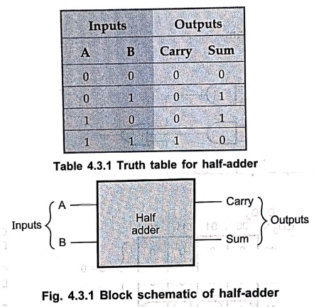
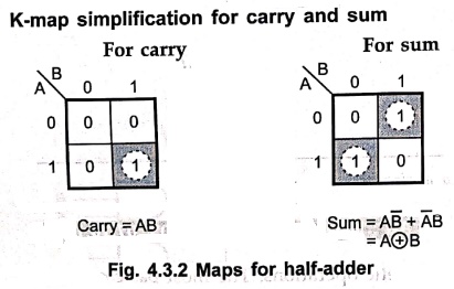
K–map simplification for carry and sum
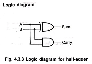
Logic diagram
half subtractor
A
half–subtractor is a combinational circuit that subtracts two–bits and produces
their difference. It also has an output to specify if a 1 has been borrowed.
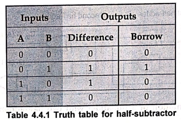
Let us designate minuend bit as A and the subtrahend bit as B. The result of
operation A – B for all possible values of A and B is tabulated in Table 4.4.1.
•
As shown in Table 4.4.1, half–subtractor has two input variables and two output
variables. The Boolean expression for the outputs of half–subtractor can be determined
as follows.
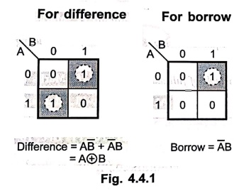
K–map simplification for half–subtractor
K–map simplification for half–subtractor
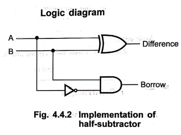
Logic diagram
7. Describe the truth table of a half subtractor and write the Boolean expression corresponding to the difference and the borrow.
A
half–subtractor is a combinational circuit that subtracts two–bits and produces
their difference. It also has an output to specify if a 1 has been borrowed.
Let us designate minuend bit as A and the subtrahend bit as B. The result of
operation A – B for all possible values of A and B is tabulated in Table 4.4.1.
•
As shown in Table 4.4.1, half–subtractor has two input variables and two output
variables. The Boolean expression for the outputs of half–subtractor can be determined
as follows.
Limitations
of half–subtractor :
In
multidigit subtraction, we have to subtract two bits along with the borrow of
the previous digit subtraction. Effectively such subtraction requires
subtraction of three bits. This is not possible with half–subtractor.
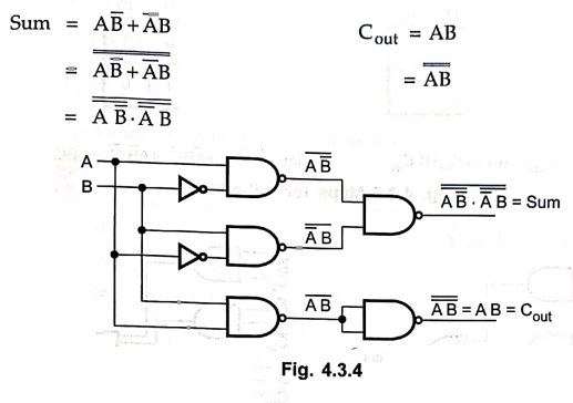
8. Implement
half adder using gates.
Draw half adder using
NAND gates.
Solution :
For half adder :
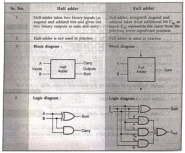
9. What
is the difference between half adder and full adder?
10. Write
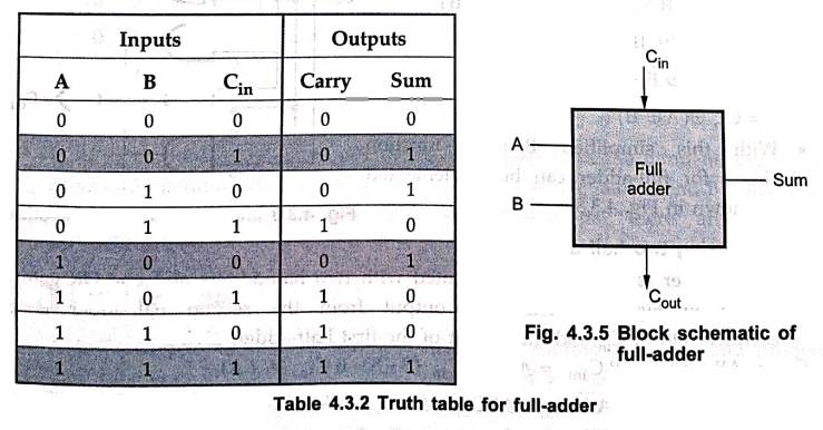
down the truth table of a full adder.
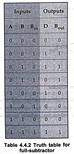
11. Write
down the truth table of a full subtractor.
12. How
will you build a full adder using 2 half adders and an OR gate ?
A full subtractor can also be implemented with two half–subtractors and one OR gate, as shown in Fig. 4.4.7. The difference output from the second half–subtractor is the exclusive–OR of Bin and the output of the first half–subtractor, which is same as difference output of full–subtractor.
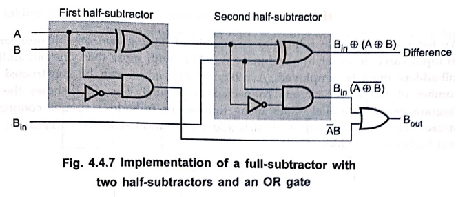
The borrow output for circuit shown in Fig. 4.4.6 can be given as,
Bout = ĀBin + ĀB + BBin
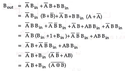
This Boolean function is same as borrow out of the full–subtractor. Therefore, we can implement full–subtractor using two half–subtractors and OR gate.
14. From
the truth table of a half subractor derive the logic equation.
15. From
the truth table of a full adder derive the logic equation.
16. From the truth table of a full subtractor derive the logic equation.
17.
Suggest a solution to overcome the limitation on the speed of an adder.
Answer: It is possible to
increase speed of adder by eliminating inter–stage carry delay. This method
utilizes logic gates to look at the lower–order bits of the augend and addend
to see if a higher–order carry is to be generated.
18. Draw
a block diagram of half adder. Write truth table. Draw logic diagram.
19. Design
a half–subtractor combinational circuit to produce the outputs. Difference and
borrow.
20. Write
the logic expressions for the difference and borrow of a half subtractor.
21. Write
an expression for borrow and difference in a full subtractor circuit.
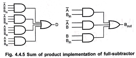
22. Draw
the logic diagram and truth table of Full adder.
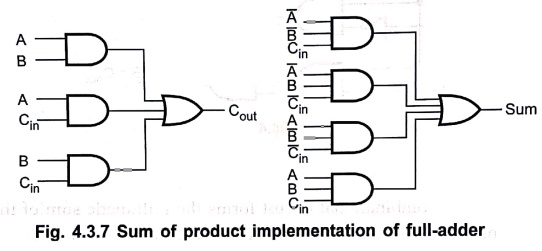
23. Draw
the full adder circuit.
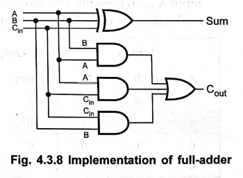
24. Draw
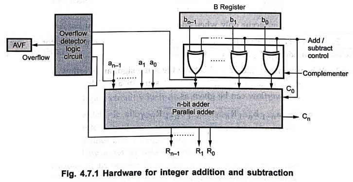
the block diagram of a 2's complement adder/subtractor.
25. What
is a data selector? or what is multiplexer ? or Why is MUX called data detector
?
Answer:
•
Multiplexer is a digital switch. Particularly, it has 2n input lines
and n selection lines whose bit combinations determine which input line is
selected and routed onto available only single output line.
•
Hence, multiplexer is a selector of one out of several data sources available
at its input lines, to connect it to output line. Simply it is a 'many into
one' device and also called 'data selector'.
26. What
is the function of the enable input in a multiplexer ?
Answer: The function of the
enable input in a MUX is to control the operation of the unit.
27. List
out the applications of multiplexer.
1.
They are used as a data selector to select one out of many data inputs.
2.
They can be used to implement combinational logic circuit.
3.
They are used in time multiplexing systems.
4.
They are used in frequency multiplexing systems.
5.
They are used in A/D and D/A converter.
6.
They are used in data acquisition systems.
28. Draw
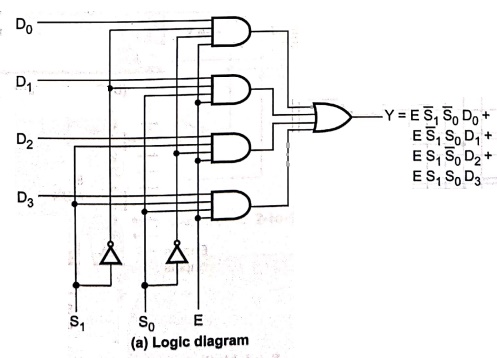
the logic diagram of a 4 line to 1 line multiplexer.
29. Draw
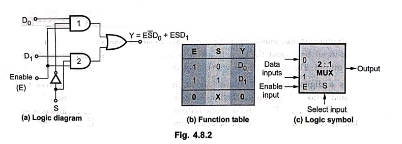
and explain the working of 2 : 1 multiplexer and realize it using basic gates.
•
When E = 0, output is 0, i.e. Y = 0 irrespective of any input condition. When E
= 1 the circuit works as follows :
•
When S = 0, the inverted S, that is 1 gets applied as second input to first AND
gate. Since S is applied directly as input to second AND gate; its output goes
zero irrespective of first input. Since the second input of first AND gate is
1, its output is equal to its first input, that is D0. Hence Y = D0.
•
Exactly opposite is the case when S = 1. In this case, second AND gate output
is equal to its first input D1 and first AND gate output is 0. Hence
Y = D1.these cases are summarized in truth table shown in Fig. 4.8.2
(b).
Deriving realization
expression
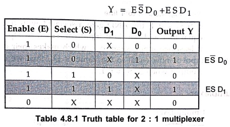
• Table 4.8.1 shows the truth table for 2 : 1 multiplexer. From the truth table it is clear that Y = 1 when E D0 = 1 or ESD1 =1 as indicated by shaded rows.
30. Write
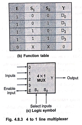
the truth table of a 4 : 1 multiplexer.
31. What
is decoder ?
Answer: A decoder is a
multiple – input, multiple–output logic circuit which converts coded inputs
into coded outputs, where the input and output codes are different. In a binary
decoder n–inputs produce 2n outputs. Usually, a decoder is provided
with enable inputs to activate decoded output.
32. What
is binary decoder ?
Answer: A decoder is a
combinational circuit that converts binary information from n input lines to a
maximum of 2n outputs lines.
33. What
will be the maximum number of outputs for a decoder with a 6 bit data word ?
Answer: 26 = 64
34. Mention
the uses of decoders.
The
uses of decoders are :
•
Code converters
•
Implementation of combinational circuits
•
Address decoding
•
BCD to 7–segment decoder
35. Distinguish
between a demultiplexer and decoder.
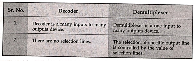
Decoder
1.
Decoder is a many inputs to many outputs device.
2.
There are no selection lines.
Demultiplexer
1.
Demultiplexer is a one input to many outputs device.
2.
The selection of specific output line is controlled by the value of selection
lines.
36. Draw
a 4 × 16 decoder constructed with two 3 × 8 decoders.
• Binary decoder circuits can be connected together to form a larger decoder circuit. Fig. 4.9.6 shows the 4 × 16 decoder using two 3 × 8 decoders.
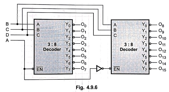
• Here, one input line (D) is used to enable/disable the decoders. When D = 0, the top decoder is enabled and the other is disabled. Thus the bottom decoder outputs are all 1s, and the top eight outputs generate minterms 0 0 0 0 to 0 1 1 1. When D =1, the enable conditions are reversed and thus bottom decoder outputs generate minterms 1000 to 1111, while the outputs of the top decoder are all 1s.
37. List
out the applications of decoder.
The
uses of decoders are :
•
Code converters
•
Implementation of combinational circuits
•
Address decoding
•
BCD to 7–segment decoder
38. Obtain
the relation between the number of inputs 'n' and outputs 'm' of a decoder.
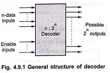
the general structure of the decoder circuit. As shown in Fig. 4.9.1, the encoded information is presented as n inputs producing 2n possible outputs. The 2n output values are from 0 through 2n – 1.
39. Convert
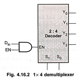
a two–to–four line decoder with enable input to 1 × 4 demultiplexer.
Answer: By driving enable
input of the decoder as shown in Fig. 4.16.2, we can convert a 2 : 4 line
decoder to 1 × 4 demultiplexer.
40. Draw
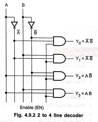
the combinational circuit that converts 2 coded inputs and 4 coded outputs.
41. What
do you mean by carry propagation delay ?
Answer:
Definition :
In parallel adders, sum and carry outputs of any stage cannot be produced until
the input carry occurs. This time delay in the addition process is called carry propagation delay. This delay
increases with increase in the number of bits to be added in an adder circuit.
42. Discuss
the principle behind the Booth's multiplier.
Answer: Booth's algorithm
generates a 2n–bit product and treats both positive and negative numbers
uniformly. This algorithm suggest that we can reduce the number of operations
required for multiplication by representing multiplier as a difference between
two numbers.
43.
Discuss the role of Booth's algorithm in the design of fast multipliers.
Answer: To speed–up the
multiplication process in the Booth's algorithm a technique called bit–pair
recoding is used. It is also called modified
Booth's algorithm. It halves the maximum number of summands. In this
technique, the Booth–recoded multiplier bits are grouped in pairs. Then each
pair is represented by its equivalent single bit multiplier reducing total
number of multiplier bits to half.
44. What
is combinational multiplier or array multiplier ?
Answer: The multiplier which
uses n shifts and adds operations to multiply n–bit binary number is called
combinational multiplier or array
multiplier.
45. What
are the two techniques for speeding up the multiplication operation?
Answer: Bit pair recoding
Carry
save addition
46. How
bit pair recoding of multiplier speeds up the multiplication process?
Answer: It guarantees that the
maximum number of summands that must be added is n/2 for n–bit operands.
47. How
CSA speeds up multiplication?
Answer: It reduces the time needed to add the
summands. Instead of letting the carries ripple along the rows, they can be
saved and introduced into the next row, at the correct waited position.
48. Write
down the steps for restoring division.
Answer: 1. Shift A and Q left
one binary position.
2.
Subtract divisor from A and place answer back in A ( A ← A – B).
3.
If the sign bit of A is 1, set Q0 to 0 and add divisor back to A
(that is, restore A); Otherwise, set Q0 to 1.
4.
Repeat steps 1, 2, and 3 n times.
49.
Define IEEE floating point single and double precision standard.
Answer: The 32–bit standard
representation (single–precision
representation) occupies a single 32–bit word. The 32–bits are divided into
three fields as shown below :
(field
1) Sign ← 1 – bit
(field
2) Exponent ←8 – bits
(field
3) Mantissa ← 23 – bits
The
64–bit standard representation (double–precision
representation) occupies two 32–bit words. The 64–bits are divided into
three fields as shown below :
(field 1) Sign ← 1 – bit
(field
2) Exponent ← 1 – bit
(field
3) Mantissa ← 52 bits
50. In
conforming to the IEEE standard mention any four situations under which a
processor sets exception flag.
Answer:
Underflow
Overflow
Divide
by zero
Inexact
Invalid
51.
Define underflow and overflow.
Answer:
Underflow : In
a single precision, if the number requires an exponent less than – 126 or in a
double precision, if the number requires an exponent less than – 1022 to
represent its normalized form the underflow occurs.
Overflow :
In a single precision, if the number requires an exponent greater than + 127 or
in a double precision, if the number requires an exponent greater than + 1023
to represent its normalized form the overflow occurs.
52. Write
down the steps for non–restoring division.
Answer:
Step 1:
If the sign of A is 0, shift A and Q left one bit position and subtract divisor
from A; otherwise, shift A and Q left and add divisor to A.
If
the sign of A is 0, set Q0 to 1; otherwise, set Q0 to 0.
Step 2 :
Repeat steps 1 and 2 for n times.
Step 3 :
If the sign of A is 1, add divisor to A.
53. What
is the advantage of non restoring over restoring division?
Answer:
Non
restoring division avoids the need for restoring the contents of register after
an successful subtraction.
54. Draw
the format of floating point number.
To represent the number in floating point format, first binary point is shifted to right of the first bit and the number is multiplied by the correct scaling factor to get the same value. The number is said to be in the normalized form and is given as
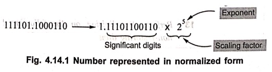
It is important to note that the base in the scaling factor is fixed 2.
55. Write
rule for addition in floating point operation.
Step 1:
Select the number with a smaller exponent and shift its mantissa right, a
number of steps equal to the difference in exponents | e2 – e1|
. For examples, if the numbers are 1.75 ×10² and 6.8 ×10⁴,
then the number 1.75 ×10² is selected and converted to 0.0175 x10⁴.
Step 2 :
Set the exponent of the result equal to the larger exponent.
Step 3 :
Perform addition/subtraction on the mantissas and determine the sign of the result.
Step 4 :
Normalize the result, if necessary.
56. State
the rules of floating point multiplication.
Answer:
1.
Add the exponents and subtract bias. (127 in case of single precision numbers
and 1023 in case of double precision numbers).
2.
Multiply the mantissas and determine the sign of the result.
3.
Normalize the result.
57. State
the rules of floating point division.
Answer:
1.
Subtract exponents and add bias (127 in case of single precision numbers and
1023 in case of double precision numbers).
2.
Divide the mantissas and determine the sign of the result.
3.
Normalize the result.
Digital Principles and Computer Organization: Chapter 4: Combinational Circuits : Tag: : Digital Principles and Computer Organization - Combinational Circuits: Two Marks Important Questions and Answers
Digital Principles and Computer Organization: Chapter 4: Combinational Circuits
Under Subject

Digital Principles and Computer Organization
CS25C06 2nd Semester AIDS, CSE, IT, CSE(CY) Dept | 2025 Regulation | 2nd Semester 2025 Regulation
Related Subjects

English Essentials II
EN25C02 2nd Semester | 2025 Regulation | 2nd Semester 2025 Regulation

Tamils and Technology தமிழர்களும் தொழில்நுட்பமும்
UC25H02 2nd Semester | 2025 Regulation | 2nd Semester 2025 Regulation

Linear Algebra
MA25C02 2nd Semester | 2025 Regulation

Applied Physics (CSIE) II
PH25C03 2nd Semester AIDS, CSE, IT, CSE(CY) Dept | 2025 Regulation | 2nd Semester 2025 Regulation
Digital Principles and Computer Organization
CS25C06 2nd Semester AIDS, CSE, IT, CSE(CY) Dept | 2025 Regulation | 2nd Semester 2025 Regulation

Basic Electrical and Electronics Engineering
EE25C01 2nd Semester | 2025 Regulation | 2nd Semester 2025 Regulation

Python for Data Science
AD25201 2nd Semester AIDS Dept | 2025 Regulation | 2nd Semester 2025 Regulation

Re-Engineering for Innovation
ME25C05 2nd Semester | 2025 Regulation | 2nd Semester 2025 Regulation

Python for Data Science - Laboratory
AD25201 2nd Semester AIDS Dept | 2025 Regulation | 2nd Semester 2025 Regulation