Digital Principles and Computer Organization: Chapter 4: Combinational Circuits
Design Procedure for Combinational Circuits
Question: Explain the design procedure for combinational circuits.
Design Procedure
•
The design of combinational circuits starts from the outline of the problem
statement and ends in a logic circuit diagram or a set of Boolean functions
from which the logic diagram can be easily obtained. The design procedure of
the combinational circuit involves following steps :
1.
The problem definition.
2.
The determination of number of available input variables and required output
variables.
3.Assigning
letter symbols to input and output variables.
4.
The derivation of truth table indicating the relationships between input and output
variables.
5.
Obtain simplified Boolean expression for each output.
6.
Obtain the logic diagram.
Example for Understanding
Example: 1
Design a combination
logic circuit with three input variables that will produce a logic 1 output
when more than one input variables are logic 1.
Solution :
Step 1:
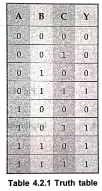
Derive the truth table for given statement.
Given
problem specifies that there are three input variables and one output variable.
We assign A, B and C letter symbols to three input variables and assign Y
letter symbol to one output variable. The relationship between input variables
and output variable can be tabulated as shown in truth Table 4.2.1.
Step 2 :
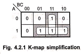
Obtain simplified Boolean expression.
Now
we obtain the simplified Boolean expression for output variable Y using K–map
simplification.
Y
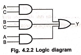
= AC + BC + AB
Step 3 :
Draw logic diagram.
In
this chapter we are going to study various combinational circuits using above
illustrated design method.
Examples with Solutions
Example: 2
A majority gate is a
digital circuit whose output is equal to 1 if the majority of inputs are 1's.
The output is 0 otherwise. Using a truth table, find the Boolean function
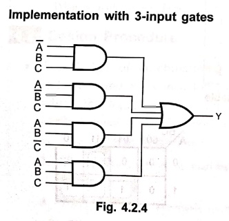
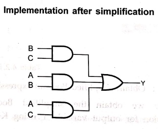
implemented by a 3–input majority gate. Simplify the function and implement
with gates.
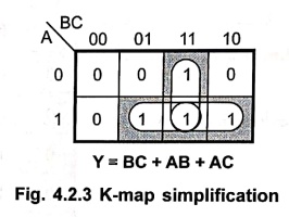
Solution :
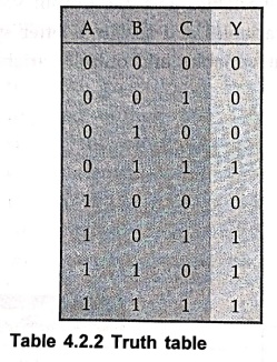
Y
= BC + AB+ AC
Implementation
after simplification
Example: 3
Design a circuit that
has one control line C and three data lines D1, D2, D3.
When the control line is high, the circuit is to detect when one of the data
lines has a 1 on it. No more than one data line will ever have a 1 on it. When
the control line is low, the circuit will output a 0, regardless of what is on
the data lines.
Solution :
The truth table for the given problem is as shown below.
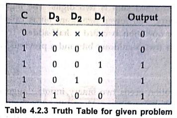
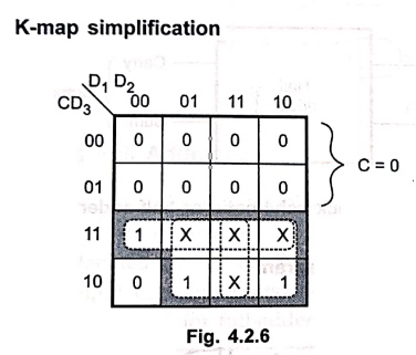
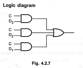
Y
= CD3 + CD2 + CD1
K–map
simplification
Logic
diagram
Review Question
1. Explain the design
procedure for combinational circuits.
Digital Principles and Computer Organization: Chapter 4: Combinational Circuits : Tag: : - Design Procedure for Combinational Circuits
Digital Principles and Computer Organization: Chapter 4: Combinational Circuits
Under Subject

Digital Principles and Computer Organization
CS25C06 2nd Semester AIDS, CSE, IT, CSE(CY) Dept | 2025 Regulation | 2nd Semester 2025 Regulation
Related Subjects

English Essentials II
EN25C02 2nd Semester | 2025 Regulation | 2nd Semester 2025 Regulation

Tamils and Technology தமிழர்களும் தொழில்நுட்பமும்
UC25H02 2nd Semester | 2025 Regulation | 2nd Semester 2025 Regulation

Linear Algebra
MA25C02 2nd Semester | 2025 Regulation

Applied Physics (CSIE) II
PH25C03 2nd Semester AIDS, CSE, IT, CSE(CY) Dept | 2025 Regulation | 2nd Semester 2025 Regulation
Digital Principles and Computer Organization
CS25C06 2nd Semester AIDS, CSE, IT, CSE(CY) Dept | 2025 Regulation | 2nd Semester 2025 Regulation

Basic Electrical and Electronics Engineering
EE25C01 2nd Semester | 2025 Regulation | 2nd Semester 2025 Regulation

Python for Data Science
AD25201 2nd Semester AIDS Dept | 2025 Regulation | 2nd Semester 2025 Regulation

Re-Engineering for Innovation
ME25C05 2nd Semester | 2025 Regulation | 2nd Semester 2025 Regulation

Python for Data Science - Laboratory
AD25201 2nd Semester AIDS Dept | 2025 Regulation | 2nd Semester 2025 Regulation