Digital Principles and Computer Organization: Chapter 4: Combinational Circuits
Multiplexer
2: 1 Multiplexer, 4: 1 Multiplexer, 8: 1 Multiplexer, Quadruple 2 to 1 Multiplex, Expanding Multiplexers, Implementation of Combinational Logic using MUX, Applications of Multiplexer, Multiplexer ICs. Questions: 1. Define multiplexer. 2. What is data selector? 3. Draw and explain the working of 2: 1 multiplexer and realize it using basic gates. 4. Explain 4 : 1 multiplexer with the help of logic circuit and truth table. 5. Write the truth table of a 4: 1 multiplexer. 6. Explain 8 : 1 multiplexer with the help of logic circuit and truth table. 7. Explain the concept and working of quadruple 2 to 1 line multiplexer. 8. State the applications of multiplexers. 9. Illustrate the concept of basic 4-input mutiplexer.
Multiplexer
•
In digital systems, many times it is necessary to select single data line from
several data–input lines, and the data from the selected data line should be
available on the output. The digital circuit which does this task is a
multiplexer.
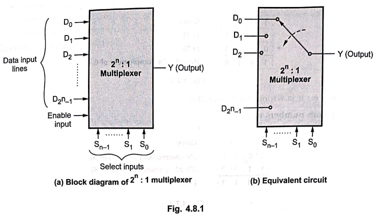
• It is a digital switch. It allows digital information from several sources to be routed onto a single output line, as shown in Fig. 4.8.1. The basic multiplexer has several data–input lines and a single output line. The selection of a particular input line is controlled by a set of selection lines. Since multiplexer selects one of the input and routes it to output, it is also known as data selector. Normally, there are 2n input lines and n selection lines whose bit combinations determine which input is selected. Therefore, multiplexer is 'many into one' and it provides the digital equivalent of an analog selector switch.
(a) Block diagram of 2n : 1 multiplexer (b) Equivalent circuit
1. 2 : 1 Multiplexer
Fig.
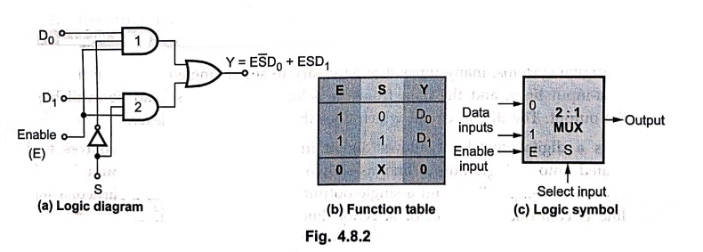
4.8.2 (a) shows 2 : 1 multiplexer. D0 is applied as an input to one
AND gate and D1 is applied as an input to another AND gate. Enable
input is applied to both gates as one input. Selection line S is connected as
second input to second AND gate. An inverted S is applied as second input to
first AND gate. Outputs of both AND gates are applied as inputs to OR gate.
(a) Logic diagram (b) Function table (c) Logic symbol
Working
•
When E = 0, output is 0, i.e. Y = 0 irrespective of any input condition. When E
= 1 the circuit works as follows :
•
When S = 0, the inverted S, that is 1 gets applied as second input to first AND
gate. Since S is applied directly as input to second AND gate; its output goes
zero irrespective of first input. Since the second input of first AND gate is
1, its output is equal to its first input, that is D0. Hence Y = D0.
•
Exactly opposite is the case when S = 1. In this case, second AND gate output
is equal to its first input D1 and first AND gate output is 0. Hence
Y = D1.these cases are summarized in truth table shown in Fig. 4.8.2
(b).
Deriving realization expression
•
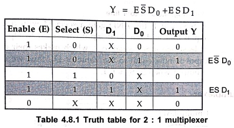
Table 4.8.1 shows the truth table for 2 : 1 multiplexer. From the truth table
it is clear that Y = 1 when E D0 = 1 or ESD1
=1 as indicated by shaded rows.
D0 = 1 or ESD1
=1 as indicated by shaded rows.
2. 4 : 1 Multiplexer
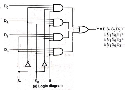
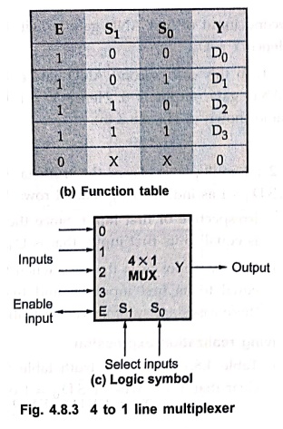
• Fig. 4.8.3 (a) shows 4–to–1 line multiplexer. Each of the four lines, D0 to D3, is applied to one input of an AND gate. Selection lines are decoded to select a particular AND gate.
(a) Logic diagram (b) Function table (c) Logic symbol
•
For example, when S1S0 = 0 1, the AND gate associated
with data input D1 has two of its inputs equal to 1 and the third
input connected to D1. The other three AND gates have at least one
input equal to 0, which makes their outputs equal to 0. The OR gate output is
now equal to the value of D1, thus we can say data bit D1
is routed to the output when S1 S0 = 0 1.
3. 8 : 1 Multiplexer
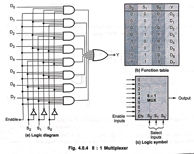
Fig. 4.8.4 shows 8 : 1 multiplexer.
(a) Logic diagram (b) Function table (c) Logic symbol
•
There are eight input lines one output line and three select lines. As shown in
the function table, the selection of a particular input line is controlled by
three and selection lines.
4. Quadruple 2 to 1 Multiplexer
•
In some cases, two or more multiplexers are enclosed within one IC package, as
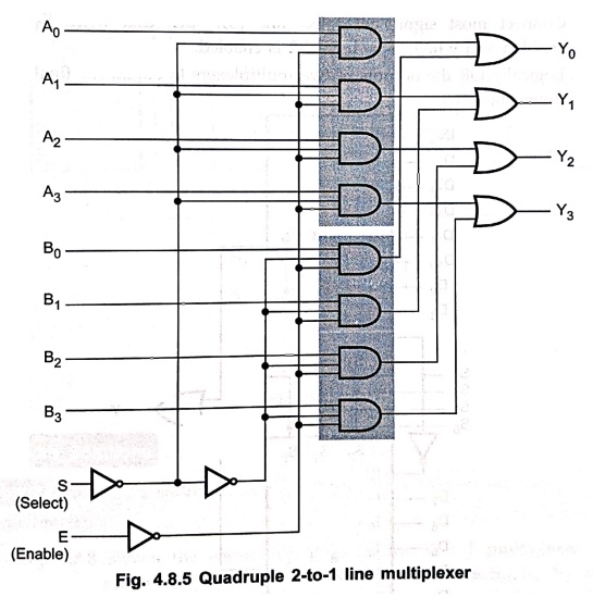
shown in Fig. 4.8.5. Fig. 4.8.5 shows quadruple 2–to–1 line multiplexer, i.e.
four multiplexers, each capable of selecting one of two input lines. Output Y1
can be selected to be equal to either A1 or B1. Similarly
output Y2 may have the value of A2 or B2, and
so on. The selection line S selects one of two lines in all four multiplexers.
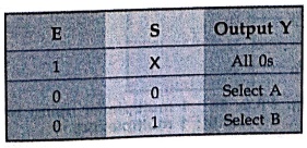
The control input E enables the multiplexers in the 0 state and disables them
in the 1 state. When E= 1, outputs have all 0's, regardless of the value of S.
Function table
5. Expanding Multiplexers
•
It is possible to expand range of inputs for multiplexer beyond the available
range by interconnecting several multiplexers in cascade. The circuit with two
or more multiplexers connected to obtain the multiplexer with more number of
inputs is known as multiplexer tree.
Examples for Understanding
Example: 1
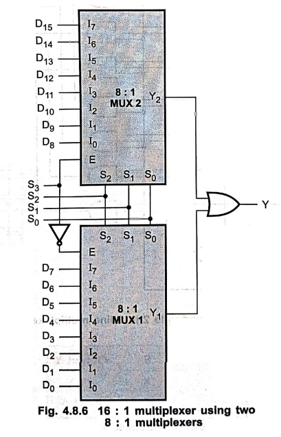
Design 16 : 1
multiplexer using 8 : 1 multiplexer.
Solution :
Step 1 : Connect
the select lines (S2, S1 and S0) of two
multiplexers in parallel.
Step 2 : Connect
most significant select line (S3) such that when S3 = 0
MUX1 is enabled and when S3 = 1, MUX2 is enabled.
Step 3 : Logically
OR the outputs of two multiplexers to obtain the final output Y. Refer Fig.
4.8.6.
Example: 2
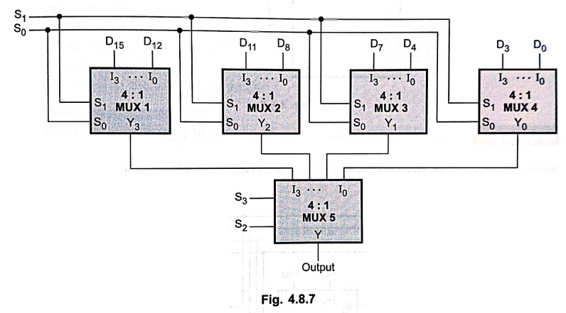
Design 16 : 1
multiplexer using 4 : 1 multiplexers.
Solution :
Since
there are 16–inputs for the multiplexers we require require four 4 : 1
multiplexers to satisfy input needs. The four outputs of 4: 1 multiplexers are
again multiplexed by 4: 1 multiplexer to generate final output.
Step 1: Connect
the select lines (S1 and S0) of four multiplexers in
parallel.
Step 2: Connect
the most significant select lines (S3 and S2) to the
MUX5.
Step 3: Connect
the outputs Y0, Y1, Y2 and Y4 of
four multiplexers as data inputs for the MUX 5, as shown in Fig. 4.8.7.
Examples with Solutions
Example: 3
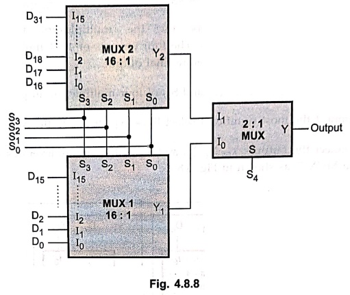
Draw 32 : 1 multiplexer
using two 16: 1 multiplexers and one 2 : 1 multiplexer.
Solution :
Fig.
4.8.8 shows the connection diagram for 32 : 1 multiplexer using two 16 : 1
multiplexer and one 2 : 1 multiplexer. Here, select lines S0, S1,
S2 and S3 are connected in parallel to 16 : 1
multiplexers and select line S4 is used to select either Y1
or Y2 using 2: 1 multiplexer.
Example: 4
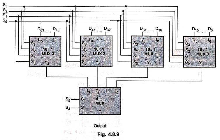
Draw 64 : 1 multiplexer
tree using 16 : 1 multiplexer.
Solution :
Fig.
4.8.9 shows 64 : 1 multiplexer using four 16 : 1 multiplexers and one 4 : 1
multiplexer.
Examples for Practice
Example: 5
Draw the block diagram
of a 4 : 1 multiplexer using 2 : 1 MUX
Example: 6
Design 32 : 1 MUX using
8 : 1 MUX.
6. Implementation of Combinational Logic using MUX
•
A multiplexer consists of a set of AND gates whose outputs are connected to
single OR gate. Because of this construction any Boolean function in a SOP form
can be easily realized using multiplexer. Each AND gate in the multiplexer
represents a minterm. In 8 to 1 multiplexer, there are 3 select inputs and 23
minterms. By connecting the function variables directly to the select inputs, a
multiplexer can be made to select the AND gate that corresponds to the minterm
in the function. If a minterm exists in a function, we have to connect the AND
gate data input to logic 1; otherwise we have to connect it to logic 0. This is
illustrated in the following example.
Examples for Understanding
Example: 7
Implement the given
function using multiplexer. F(x,y,z) = (0,2,6,7).
Solution :
Step 1: Select
the multiplexer. Here, Boolean expression has 3 variables, thus we require 23
= 8: 1 multiplexer.
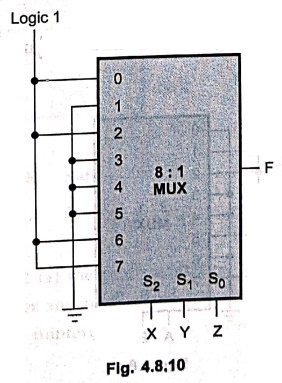
Step 2 :
Connect inputs corresponds to the present minterms to logic 1.
Step 3 : Connect
remaining inputs to logic 0.
Step 4 : Connect
input variables to select lines of MUX.
Example: 8
Implement the Boolean
function represented by the given truth table using multiplexer.
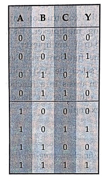
Solution :
Step 1: Select
the multiplexer. Here, there are three input variables, thus we require 23
= 8 : 1 multiplexer.
Step 2 :
Find the minterm expression.
Minterm
expression for given truth table is Σ m (1, 2, 5, 7).
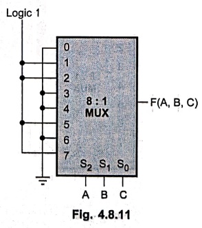
Step 3 :
Connect inputs corresponds to the present minterms to logic 1.
Step 4 :
Connect remaining inputs to logic 0.
Step 5 : Connect
input variables to select lines of MUX.
•
In the above example, we have seen the method for implementing Boolean function
of 3 variables with 23(8) – to –1 multiplexer. Similarly, we can
implement any Boolean function of n variables with 2n–to–1
multiplexer. However, it is possible to do better than this. If we have Boolean
function of n + 1 variables, we take n of these variables and connect them to
the selection lines of a multiplexer. The remaining single variable of the
function is used for the inputs of the multiplexer. In this way we can
implement any Boolean function of n variables with 2n–1–to–1
multiplexer. Let us see some example.
Example: 9
Implement the following
Boolean function using 4: 1 multiplexer. F (A, B, C) = Σ m (1, 3, 5, 6).
Solution :
Step
1:
Connect least significant variables as a variables as a select inputs of
multiplexer. Here, connect C to S0
and B to S1.brobable
Step 2 :
Derive inputs for multiplexer using implementation table.
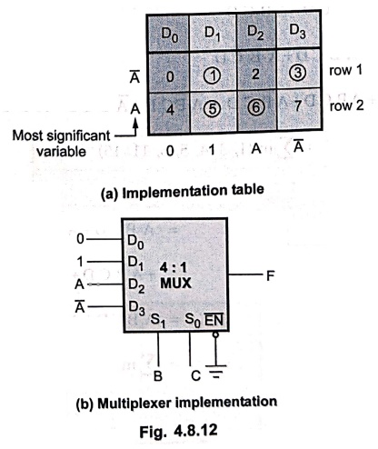
•
As shown in Fig. 4.8.12 (a) the implementation table is nothing but the list of
the inputs of the multiplexer and under them list of all the minterms in two
rows. The first row lists all those minterms where A is complemented, and the
second row lists all the minterms with A uncomplemented. The minterms given in
th function are circled and then each column is inspected separately as follows
:
■
If the two minterms in a column are not circled, 0 is applied to the
corresponding multiplexer input (see column 0).
■
If the two minterms in a column are circled, 1 is applied to the corresponding
multiplexer input (see column 1).
■
If the minterm in the second row is circled and minterm in the first row is not
circled, A is applied to the corresponding multiplexer input (see column 2).
■
If the minterm in the first row is circled and minterm in the second row is not
circled, Ā is applied to the corresponding multiplexer input (see column 3).
Example: 10
Implement the following
Boolean function using 8 : 1 multiplexer 
Solution :
Step 1:
Express Boolean function in the minterm form.
The
given Boolean expression is not in standard SOP form. Let us first convert this
in standard SOP form
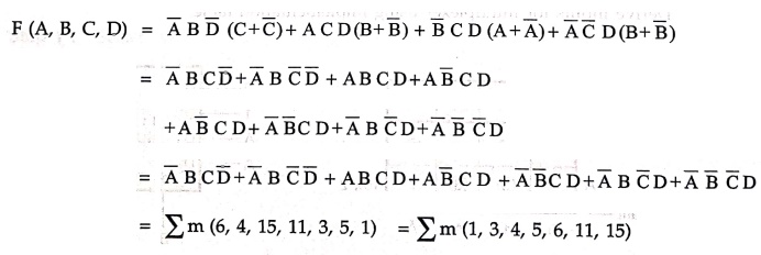
=
Σ m (6, 4, 15, 11, 3, 5, 1) = Σ m (1, 3, 4, 5, 6, 11, 15)
Step 2 :
Implement it using implementation table.
From
the Boolean function in the minterm form can be implemented using 8 :1
multiplexer as follows :
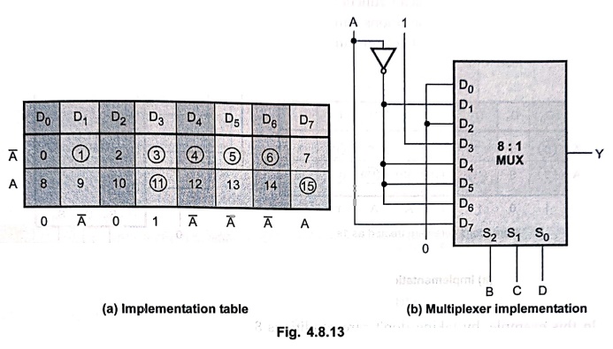
Example: 11
Implement the following
Boolean function with 8: 1 multiplexer
F(A, B, C, D) = π M (0,
3, 5, 8, 9, 10, 12, 14).
Solution :
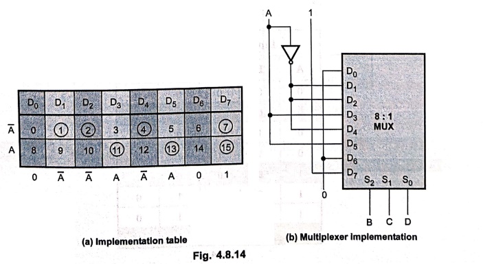
Here,
instead of minterms, maxterms are specified. Thus, we have to circle maxterms
which are not included in the Boolean function. Fig. 4.8.14 shows the
implementation of Boolean function with 8:1 multiplexer.
Example: 12
Implement the following
Boolean function with 8 : 1 multiplexer.
F(A, B, C, D) = Σ m (0,
2, 6, 10, 11, 12, 13) + d (3, 8, 14).
Solution :
In
the given Boolean function three don't care conditions are also specified. We
know that don't care conditions can be treated as either 0s or 1s. Fig. 4.8.15
shows the implementation of given Boolean function using 8 : 1 multiplexer.
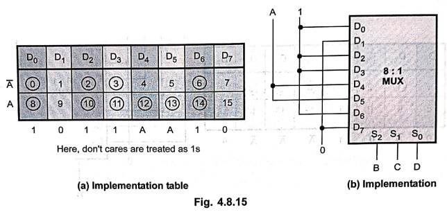
In
this example, by taking don't care conditions 8 and 14 as 1s we have eliminated
Ā term and hence the inverter.
Examples with Solutions
Example: 13
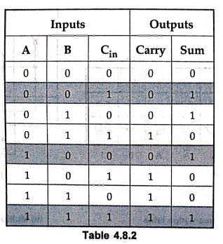
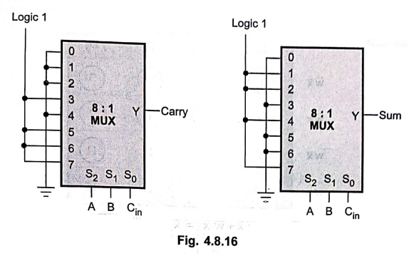
Implement full adder
circuit using 8 : 1 multiplexer.
Solution :
Example: 14
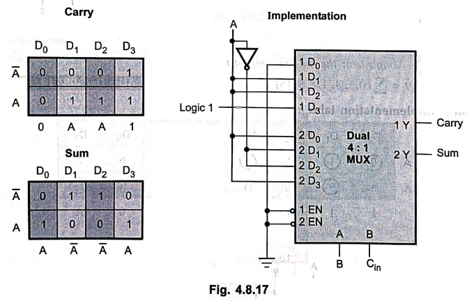
Implement full adder
circuit using dual 4 to 1 multiplexer.
Solution :
Implementation tables :
Example: 15
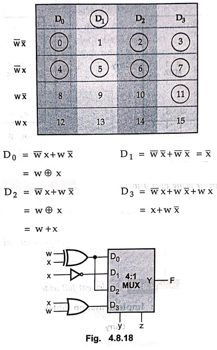
Realize F(w, x, y, z) =
Σ (1, 4, 6, 7, 8, 9, 10, 11, 15) using 4 to 1 MUX.
Solution :
Example: 16
Implement the function
with a multiplexer.
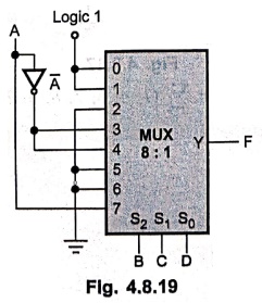
F(A, B, C, D) = Σ (0,1,3,4,8,9,15)
Solution :
Implementation table :
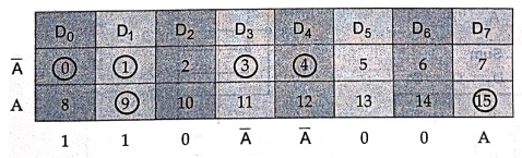
Implementation
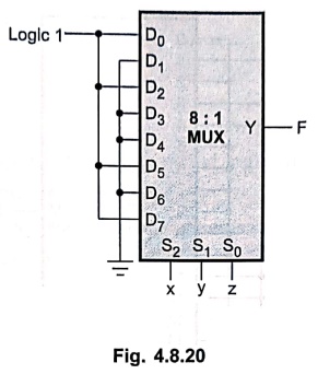
Example: 17
Implement the following
function using suitable multiplexer. F(x, y, z) = Σ m (0, 2, 5, 7).
Solution :
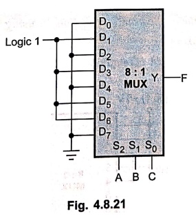
Example:
18
Implement the given
Boolean function using 8 : 1 multiplexer.
F(A, B, C) = Σ (1, 3,
5, 6).
Solution :
Example: 19
Implement the following
function using suitable multiplexer
F(A, B, C, D) = Σ (1,
3, 4, 11, 12, 13, 14, 15).
Solution :
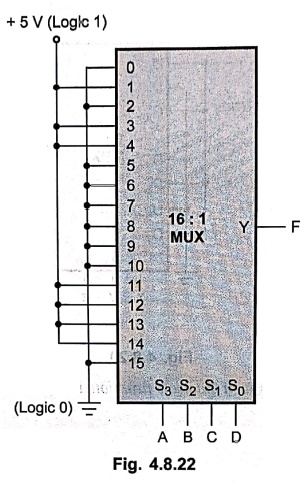
Example: 20
Realize the Boolean
function using appropriate multplexer
F(A, B, C) = Σ (0, 1, 3, 7).
Solution :
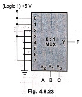
Examples
with practice
Example: 21
Implement the following
function using 8:1 multiplexer f(a, b, c, d) = Σ m (0, 1, 5, 6, 8, 10, 12, 15)
Example: 22
Implement Boolean
function f = AB +  D + A
D + A C using 8 : 1 multiplexer.
7. Applications of Multiplexer
1.
They are used as a data selector to select one out of many data inputs.
2.
They can be used to implement combinational logic circuit.
3.
They are used in time multiplexing systems.
4.
They are used in frequency multiplexing systems.
5.
They are used in A/D and D/A converter.
6.
They are used in data acquisition systems.
8. Multiplexer ICs
IC number – Function
74150 – 16:
1 multiplexer
74151 – 8: 1 multiplexer
74153 – Dual 4: 1 multiplexer
74157 – Quad
2–input multiplexer
Review Questions
1. Define multiplexer.
2. What is data
selector?
3. Draw and explain
the working of 2 : 1 multiplexer and realize it using basic gates.
4. Explain 4 : 1
multiplexer with the help of logic circuit and truth table.
5. Write the truth
table of a 4: 1 multiplexer.
6. Explain 8 : 1
multiplexer with the help of logic circuit and truth table.
7. Explain the concept
and working of quadruple 2 to 1 line multiplexer.
8. State the
applications of multiplexers.
9. Illustrate the
concept of basic 4–input mutiplexer.
Digital Principles and Computer Organization: Chapter 4: Combinational Circuits : Tag: : - Multiplexer
Digital Principles and Computer Organization: Chapter 4: Combinational Circuits
Under Subject

Digital Principles and Computer Organization
CS25C06 2nd Semester AIDS, CSE, IT, CSE(CY) Dept | 2025 Regulation | 2nd Semester 2025 Regulation
Related Subjects

English Essentials II
EN25C02 2nd Semester | 2025 Regulation | 2nd Semester 2025 Regulation

Tamils and Technology தமிழர்களும் தொழில்நுட்பமும்
UC25H02 2nd Semester | 2025 Regulation | 2nd Semester 2025 Regulation

Linear Algebra
MA25C02 2nd Semester | 2025 Regulation

Applied Physics (CSIE) II
PH25C03 2nd Semester AIDS, CSE, IT, CSE(CY) Dept | 2025 Regulation | 2nd Semester 2025 Regulation
Digital Principles and Computer Organization
CS25C06 2nd Semester AIDS, CSE, IT, CSE(CY) Dept | 2025 Regulation | 2nd Semester 2025 Regulation

Basic Electrical and Electronics Engineering
EE25C01 2nd Semester | 2025 Regulation | 2nd Semester 2025 Regulation

Python for Data Science
AD25201 2nd Semester AIDS Dept | 2025 Regulation | 2nd Semester 2025 Regulation

Re-Engineering for Innovation
ME25C05 2nd Semester | 2025 Regulation | 2nd Semester 2025 Regulation

Python for Data Science - Laboratory
AD25201 2nd Semester AIDS Dept | 2025 Regulation | 2nd Semester 2025 Regulation