Digital Principles and Computer Organization: Chapter 4: Combinational Circuits
Design of Fast Adder
Questions: 1. What do you mean by carry propagation delay? 2. Explain the method used for fast addition (carry look ahead generation). 3. Relate carry generate, carry propagate, sum and carry-out of a carry look ahead adder. 4. Explain the concept of carry look ahead adder with neat logic diagram.
Design of Fast Adder
•
The parallel adder discussed in the last paragraph is ripple carry type in
which the carry output of each full–adder stage is connected to the carry input
of the next higher–order stage. Therefore, the sum and carry outputs of any
stage cannot be produced until the input carry occurs; this leads to a time
delay in the addition process. This delay is known as carry propagation delay,
which can be best explained by considering the following addition.
0 1 0 1
+ 0 0 1
1
––––––
1 0 0 0
•
Addition of the LSB position produces a carry into the second position. This carry,
when added to the bits of the second position (stage), produces a carry into
the third position. The latter carry, when added to the bits of the third
position, produces a carry into the last position. The key thing to notice in
this example is that the sum bit generated in the last position (MSB) depends
on the carry that was generated by the addition in the previous positions. This
means that, adder will not produce correct result until LSB carry has
propagated through the intermediate full–adders. This represents a time delay
that depends on the propagation delay produced in an each full–adder. For
example, if each full–adder is considered to have a propagation delay of 30 ns,
then S3 will not reach its correct value until 90 ns after LSB carry
is generated. Therefore, total time Dipol required to perform addition is 90 + 30
= 120 ns.
•
Obviously, this situation becomes much worse if we extend the adder circuit to
add a greater number of bits. If the adder were handling 16–bit numbers, the
carry propagation delay could be 480 ns.
•
One method of speeding up this process by eliminating inter stage carry delay
is called look ahead–carry addition. This method utilizes logic gates to look at
the lower–order bits of the augend and addend to see if a higher–order carry is
to be generated. It uses two functions : carry generate and carry propagate.
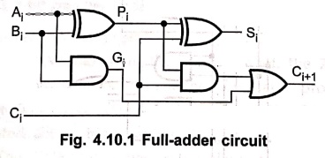
Consider
the circuit of the full–adder shown in Fig. 4.10.1. Here, we define two
functions : carry generate and carry propagate.
Pi
= Ai ⊕
Bi
Gi
= AiBi
The
output sum and carry can be expressed as
Si = Pi ⊕ Ci
Ci+1
= Gi + PiCi
•
Gi is called a carry generate
and it produces on carry when both Ai and Bi are one, regardless
of the input carry. Pi is called a carry propagate because it is
term associated with the propagation of the carry from Ci to Ci+1.
Now
the Boolean function for the carry output of each stage can be written as
follows.
C2
= G1 + P1C1
C3
= G2+ P2C2 = G2 + P2 (G1
+ P1C1)
= G2+P2G1
+ P2 P1C1
C4
= G3 + P3C3
= G3 + P3 (G2 +
P2G1 + P2P1C1)
= G3+ P3G2+
P3 P2 G1 + P3 P2 P1
C1
From
the above Boolean function it can be seen that C4 does not have to
wait for C3 and C2 to propagate; in fact C4 is
propagated at the same time as C2 and C3.
•
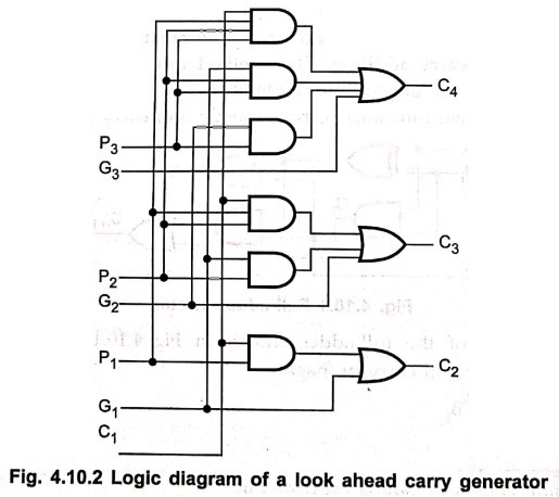
The Boolean functions for each output carry are expressed in sum–of product
form, thus they can be implemented using AND–OR logic or NAND–NAND logic. Fig.
4.10.2 shows implementation of Boolean functions for C2, C3
and C4 using AND–OR logic.
•
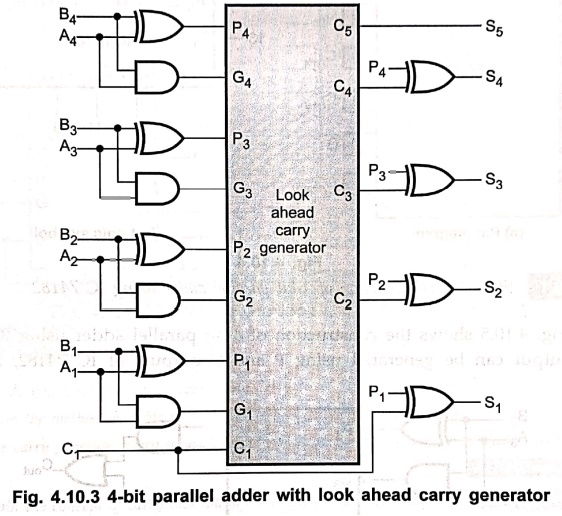
Using a look ahead carry generator we can easily construct a 4–bit parallel
adder with a look ahead carry scheme. Fig. 4.10.3 shows a 4–bit parallel adder
with a look ahead carry scheme. As shown in Fig. 4.10.3, each sum output
requires two exclusive–OR gates. The output of first exclusive–OR gate
generates Pi , and the AND gate generates Gi. The carries
are generated using look ahead carry generator and applied as inputs to the
second exclusive–OR gate. Other inputs to exclusive–OR gate is Pi.
Thus second exclusive–OR gate generates sum outputs. Each output each generated
after a delay of two levels of gate. Thus outputs S2 through S4
have equal propagation delay times.
•
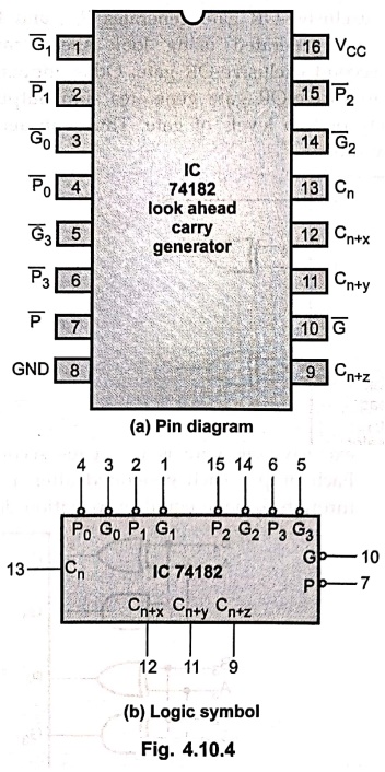
IC 74182 is a look ahead carry generator. Fig. 4.10.3 shows pin diagram and
logic symbol for IC 74182. As shown in the logic symbol, the 74182 carry look
ahead generator accepts up to four pairs of active low carry propagate 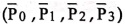 and carry generate
  signals and an active high carry
input (Cn) and provides anticipated active high carries (Cn+x,
Cn+y, Cn+z) across four groups of binary adders. The
74182 also has active low carry propagate (
signals and an active high carry
input (Cn) and provides anticipated active high carries (Cn+x,
Cn+y, Cn+z) across four groups of binary adders. The
74182 also has active low carry propagate ( ) and carry generate
(
) and carry generate
( ) outputs which may be used for further levels of look ahead.
•The
logic equations provided at the outputs of 74182 are :
Cn+x
= G0 + P0 Cn
Cn+y
= G1+ P1 G0 + P1 P0
Cn
Cn+z
= G2+ P2 G1 +P2 P1
G0

(a) Pin diagram (b) Logic symbol
Example: 1
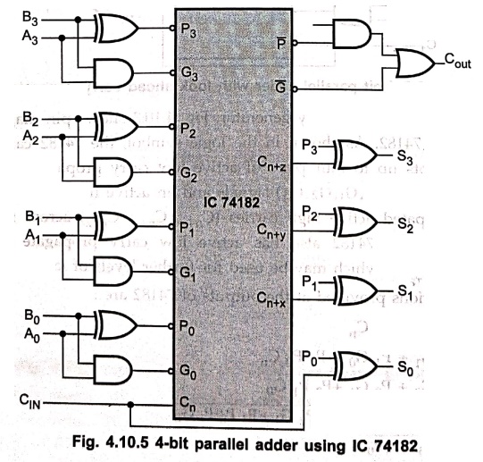
Show the construction
of 4–bit parallel adder using IC 74182.
Solution :
Fig.
4.10.5 shows the construction of 4–bit parallel adder using IC 74182. The last
carry output can be generated using and outputs
of IC 74182, as shown in Fig. 4.10.5.
Example: 2
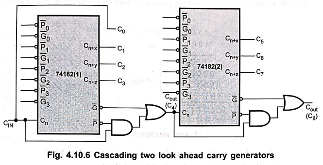
Construct the look
ahead carry generator to accommodate higher word size.
Solution :
Look
ahead carry generators can be cascaded to increase the word size in multiples
of 4–bits. Fig. 4.10.6 shows the cascading two look ahead carry generators (IC
74182s) to get word size of 8–bits.
Review Questions
1. What do you mean by
carry propagation delay?
2. Explain the method
used for fast addition (carry look ahead generation).
3. Relate carry
generate, carry propagate, sum and carry–out of a carry look ahead adder.
4. Explain the concept
of carry look ahead adder with neat logic diagram.
Digital Principles and Computer Organization: Chapter 4: Combinational Circuits : Tag: : - Design of Fast Adder
Digital Principles and Computer Organization: Chapter 4: Combinational Circuits
Under Subject

Digital Principles and Computer Organization
CS25C06 2nd Semester AIDS, CSE, IT, CSE(CY) Dept | 2025 Regulation | 2nd Semester 2025 Regulation
Related Subjects

English Essentials II
EN25C02 2nd Semester | 2025 Regulation | 2nd Semester 2025 Regulation

Tamils and Technology தமிழர்களும் தொழில்நுட்பமும்
UC25H02 2nd Semester | 2025 Regulation | 2nd Semester 2025 Regulation

Linear Algebra
MA25C02 2nd Semester | 2025 Regulation

Applied Physics (CSIE) II
PH25C03 2nd Semester AIDS, CSE, IT, CSE(CY) Dept | 2025 Regulation | 2nd Semester 2025 Regulation
Digital Principles and Computer Organization
CS25C06 2nd Semester AIDS, CSE, IT, CSE(CY) Dept | 2025 Regulation | 2nd Semester 2025 Regulation

Basic Electrical and Electronics Engineering
EE25C01 2nd Semester | 2025 Regulation | 2nd Semester 2025 Regulation

Python for Data Science
AD25201 2nd Semester AIDS Dept | 2025 Regulation | 2nd Semester 2025 Regulation

Re-Engineering for Innovation
ME25C05 2nd Semester | 2025 Regulation | 2nd Semester 2025 Regulation

Python for Data Science - Laboratory
AD25201 2nd Semester AIDS Dept | 2025 Regulation | 2nd Semester 2025 Regulation