Digital Principles and Computer Organization: Chapter 4: Combinational Circuits
Decoders
1. Binary Decoder, 2 The 74X138 3-to-8 Decoder, 3 The 74X139 Dual 2 to 4 Decoder, 4 Expanding Cascading Decoders, 5 Realization of Boolean Function using Decoder, 6 Applications of Decoder, 7 Decoder ICs, 8 BCD to Decimal Decoder, 9 BCD to Seven Segment Decoder. Questions: 1. Define decoder. 2. Define binary decoder. 3. Explain the working of 2: 4 binary decoder. 4. Draw a 4 × 16 decoder constructed with two 3 × 8 decoders. 5. State the procedure to implement Boolean function using decoder. 6. Mention the uses of decoders. 7. Draw the logic diagram of BCD - Decimal decoder and explain its operations. 8. Write a note on BCD to 7-segment decoder.
Decoders
•
A decoder is a multiple–input, multiple–output logic circuit which converts
coded inputs into coded outputs, where the input and output codes are
different.
•
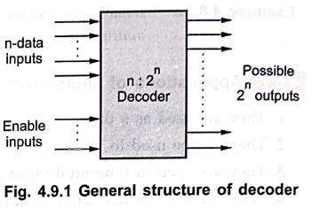
Fig. 4.9.1 shows the general structure of the decoder circuit. As shown in Fig.
4.9.1, the encoded information is presented as n inputs producing 2n
possible outputs. The 2n output values are from 0 through 2n –
1.
•
Usually, a decoder is provided with enable inputs to activate decoded output
based on data inputs. When any one enable input is unasserted, all outputs of
decoder are disabled.
1. Binary Decoder
•
A decoder which has an n–bit binary input code and a one activated output out
of 2n output code is called binary
decoder. A binary decoder is used when it is necessary to activate exactly
one of 2n outputs based on an n–bit input value.
•
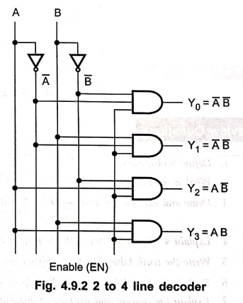
Fig. 4.9.2 shows 2 to 4 decoder. Here, 2 inputs are decoded into four outputs,
each output representing one of the minterms of the 2 input variables. The two
inverters provide the complement of the inputs, and each one of four AND gates
generates one of the minterms.
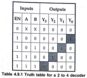
Table
4.9.1 shows the truth table for a 2 to 4 decoder. As shown in the truth table,
if enable input is 1 (EN = 1), one, and only one, of the outputs Y0
to Y3, is active for a given input. The output Y0 is
active, i.e. Y0 =1 when inputs A = B = 0, the output Y1
is active when inputs A = 0 and B = 1. If enable input is 0, i.e. EN = 0, then
all the outputs are 0.
Example: 1
Draw the circuit for 3
to 8 decoder and explain.
Solution :
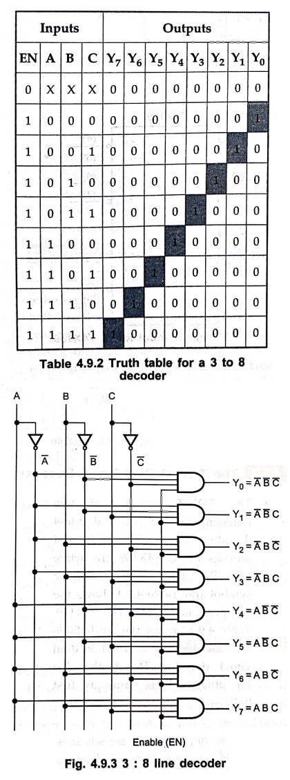
Fig. 4.9.3 shows 3 to 8 line decoder. Here, 3 inputs are decoded into eight
outputs, each output represent one of the minterms of the 3 input variables.
The three inverters provide the complement of the inputs, and each one of the
eight AND gates generates one of the minterms. Enable input is provided to
activate decoded output based on data inputs A, B, and C. The table shows the
truth table for 3 to 8 decoder.
2. The 74X138 3–to–8 decoder
•
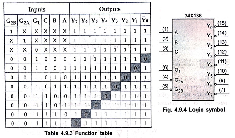
The 74X138 is a commercially available 3–to–8 decoder. It accepts three binary
inputs (A, B, C) and when enabled, provides eight individual active low outputs
(Y0 – Y7). The device has three enable inputs : two
active low  and one active high (G1). Fig. 4.9.4
and Table 4.9.3 show logic symbol and function table respectively.
and one active high (G1). Fig. 4.9.4
and Table 4.9.3 show logic symbol and function table respectively.
3. The 74X139 Dual 2 to 4 Decoder
•
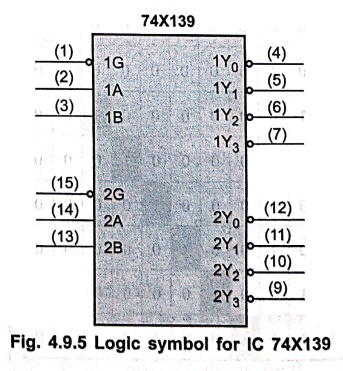
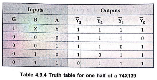
The 74X139 consists of two independent and identical 2–to–4 decoders. The
enable inputs and outputs of IC 74X139 are active low. Fig. 4.9.5 shows the
logic symbol and Table 4.9.4 shows the 58A function table for IC 74X139. Table
4.9.4 shows the truth table Afor one half of a 74X139 dual 2–to–4 decoder. The
truth table for other half is same as first half.
4. Expanding Cascading Decoders
•
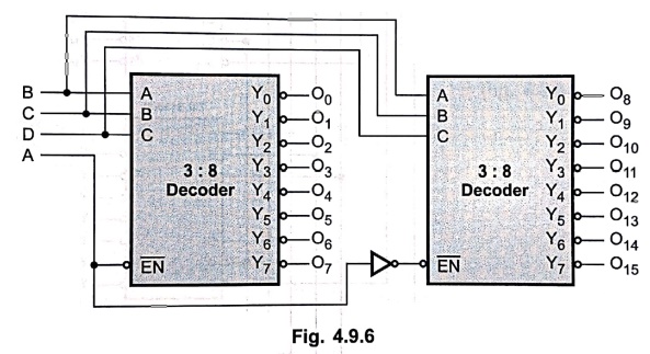
Binary decoder circuits can be connected together to form a larger decoder circuit.
Fig. 4.9.6 shows the 4 × 16 decoder using two 3 × 8 decoders.
•
Here, one input line (D) is used to enable/disable the decoders. When D = 0,
the top decoder is enabled and the other is disabled. Thus the bottom decoder
outputs are all 1s, and the top eight outputs generate minterms 0 0 0 0 to 0 1
1 1. When D =1, the enable conditions are reversed and thus bottom decoder
outputs generate minterms 1000 to 1111, while the outputs of the top decoder
are all 1s.
Example: 2
Design 5–to–32 decoder
using one 2–to–4 and four 3–to–8 decoder ICs.
Solution :
Fig.
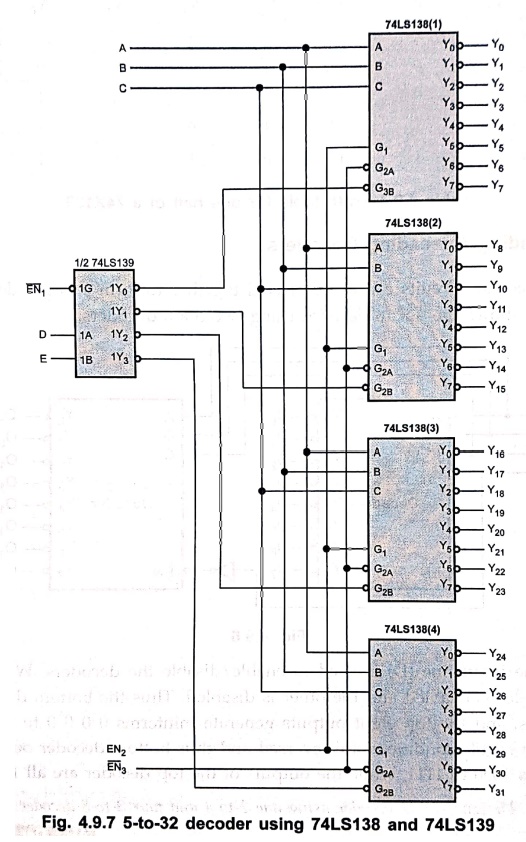
4.9.7 shows the construction of 5–to–32 decoder using four 74LS138s and half
74LS139. The half section of 74LS139 IC is used as a 2–to–4 decoder to decode
the two higher order inputs, D and E. The four outputs of this decoder are used
to enable one of the four 3 to 8 decoders. The three lower order inputs A, B
and C are connected in parallel to four 3 to 8 decoders. This means that the
same output pin of each of the four 3–to–8 decoders is selected but only one is
enabled. The remaining enable signals of four 3–to–8 decoder ICs are connected
in parallel to construct enable signals for 5–to–32 decoder.
5. Realization of Boolean Function using Decoder
•
The combination of decoder and external logic gates can be used to implement
single or multiple output functions. We know that decoder can have one of the two
output states; either active low or active high. Let us see the significance of
if these output states in the implementation of binary function.
•
When decoder output is active high, it generates minterms (product terms) for
input variables; i.e. it makes selected output logic 1. In such case to
implement SOP function we have to take sum of selected product terms generated
by decoder.
Examples for Understanding
Example: 3
Implement Boolean
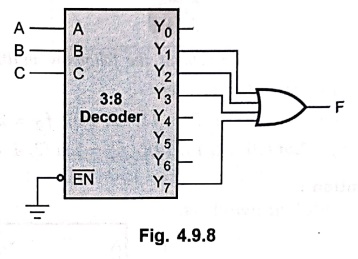
function F = m (1, 2, 3, 7) using 3: 8 decoder.
Solution:
Step 1:
Connect function variables inputs to the decoder.
Step 2 :
Logically OR the outputs correspond to present minterms to obtain the output.
Example: 4
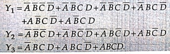
Implement the following
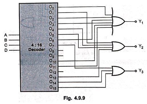
multiple output combinational logic using a 4 line to 16 line decoder.
Solution :
Step 1:
Write the function in their minterm forms
Y1
= Σ m (0, 3, 2, 6, 10, 11)
Y2
= Σ m (1, 4, 5, 13)
Y3
= Σ m (7, 14, 15)
Step 2 :
Logically OR the outputs of decoder corresponding to the minterms in the functions.
Examples with Solutions
Examples:
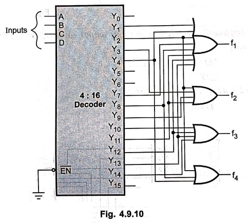
5
Implement the following
multiple output combinational logic circuit using a 4–line to 16–line decoder.
f1 = Σ m (1, 2, 4, 7, 8, 11, 12, 13),
f2 = Σm (2, 3, 9, 11)
f3= Σ m (10, 12, 13, 14),
f4 = Σ m (2, 4, 8)
Solution :
Example: 6
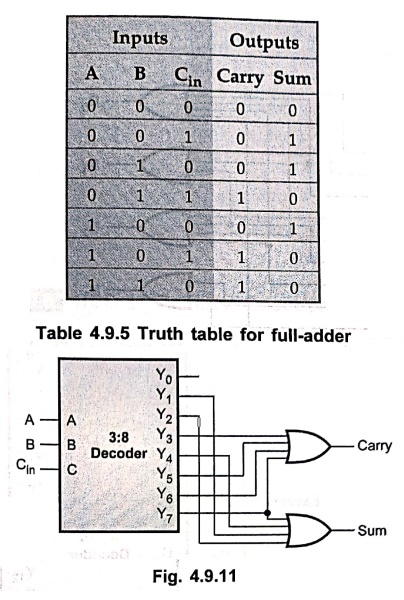
Design and implement a
full adder circuit using a 3 : 8 decoder.
Solution :
The
truth table for full adder as shown in Table 4.9.5.
Example: 7
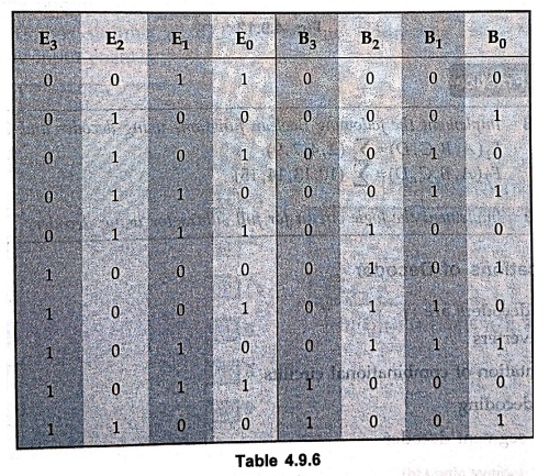
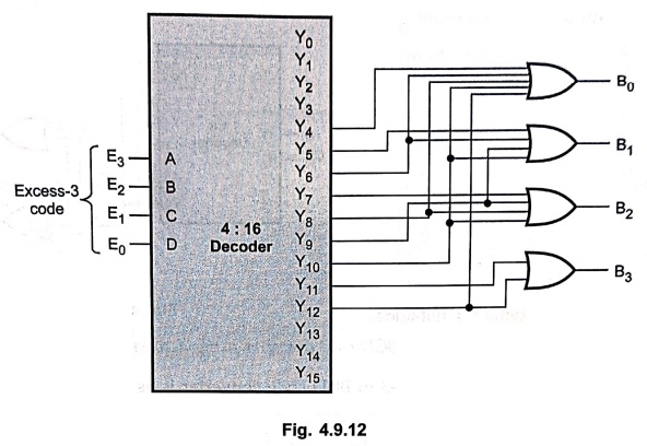
Design an excess–3 to
BCD code converter using decoder and gates.
Solution :
The
truth table for excess–3 to BCD code converter is as shown in Table 4.9.6.
Realization
Examples for Practice
Example: 8
Implement the following
Boolean functions using decoder and OR gates :
F1(A,B,C,D) =
Σ (2,4,7,9)
F2(A,B,C,D) =Σ
(10,13,14,15)
Example: 9
Implement the logic
circuit for full subtractor using decoder.
6. Applications of Decoder
The
uses of decoders are :
•
Code converters
•
Implementation of combinational circuits
•
Address decoding
•
BCD to 7–segment decoder
7. Decoder ICs
IC Number – Function
74138 –
3 : 8 Decoder
74139 –
Dual 2 : 4 Decoder
7442 – BCD to decimal decoder
7447 – BCD to 7–segment decoder
8. BCD to Decimal Decoder
•
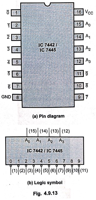
BCD decoders have four inputs and 10 outputs. The four–bit BCD input is decoded
to activate one of the ten outputs. The 74XX42 is a BCD to decimal decoder. It
accepts four active high BCD inputs and provides 10 independent active low
outputs. Fig. 4.9.13 (a) shows pin diagram and logic symbol for IC 7442. The
active low outputs of IC 7442 facilitates addressing other MSI units with
active low input enables.
•
The logic design of 7442 ensures that all outputs are high when binary codes
greater than nine are applied to the inputs. The most significant input, A3
produces a useful inhibit function when the 7442 is used as a 3 to 8 decoder.
•
The IC 7445 is also a BCD to decimal decoder with identical pin description as
that of IC 7442. However, IC 7445 provides open collector outputs.
9. BCD to Seven Segment Decoder
•
In
most practical applications, seven segment displays are used to give a visual
indication of the output states of digital ICs such as decade counters, latches
etc. These outputs are usually in four bit BCD (binary coded decimal) form, and
are thus not suitable for directly driving seven segment displays. The special
BCD to seven segment decoder/driver ICs are used to convert the BCD signal into
a form suitable for driving these displays. In this sections, we are going to
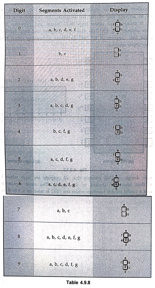
study LED and LCD decoders/drivers for seven segment displays. Let us tabulate
the segments activated during each digit display.
•
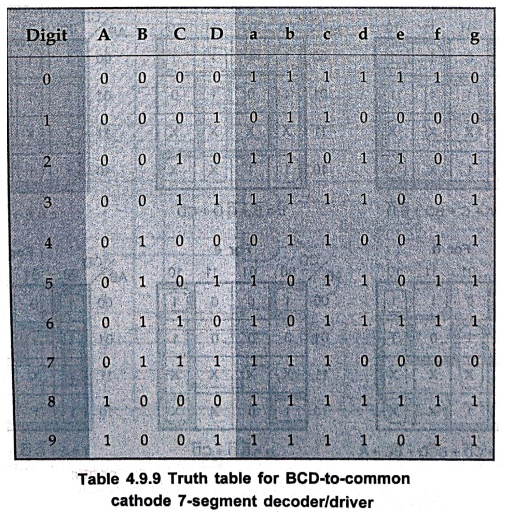
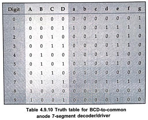
From Table 4.9.8 we can determine the truth table for BCD–to–7 segment
decoder/driver. This truth table also depends on the construction of 7–segment
display. If 7–segment display is common anode, the segment driver output must
be active low to glow the segment. In case of common cathode type 7–segment
display, the segment driver output must be active high to glow the segment.
Table 4.9.9 and 4.9.10 show the truth tables for both BCD to 67 segment
decoder/driver with common cathode display and with common anode display
respectively.
•
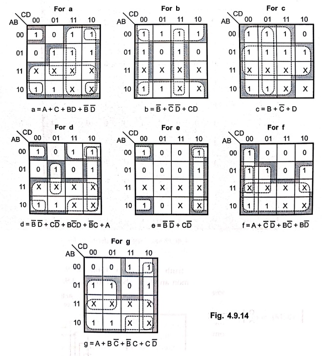
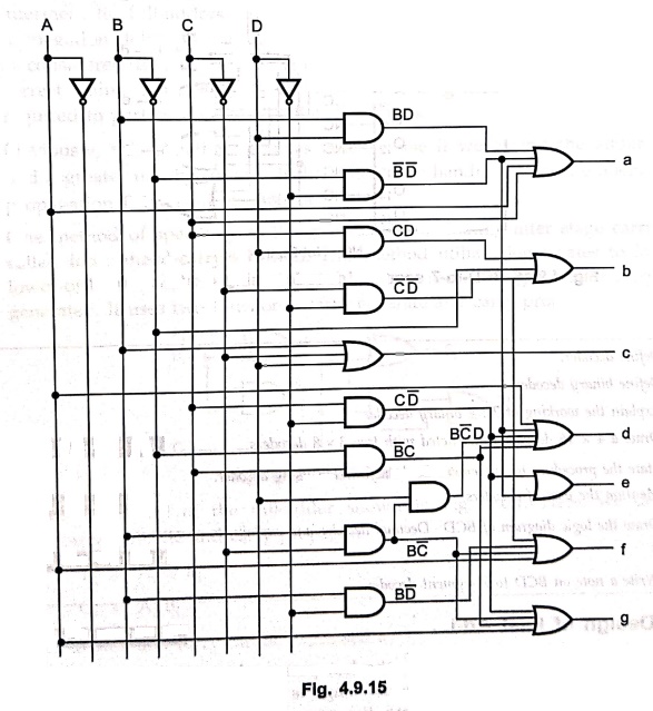
Let us design the combinational circuit for common cathode 7–segment
display/driver.
K–map simplification
Logic diagram
Example: 10
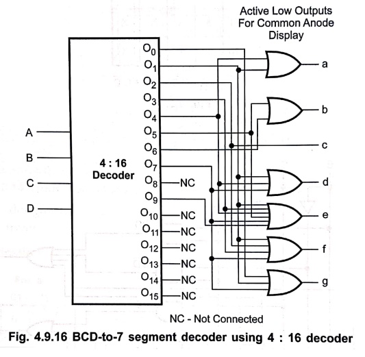
Implement BCD–to–7
segment decoder for common anode using 4 : 16 decoder.
Solution :
Referring
the truth table from Table 4.9.9 we can implement BCD–to–7 segment decoder for
common anode as shown in Fig. 4.9.16.
Review Questions
1. Define decoder.
2. Define binary
decoder.
3. Explain the working
of 2: 4 binary decoder.
4. Draw a 4 × 16 decoder
constructed with two 3 × 8 decoders.
5. State the procedure
to implement Boolean function using decoder.
6. Mention the uses of
decoders.
7. Draw the logic diagram
of BCD – Decimal decoder and explain its operations.
8. Write a note on BCD
to 7–segment decoder.
Digital Principles and Computer Organization: Chapter 4: Combinational Circuits : Tag: : - Decoders
Digital Principles and Computer Organization: Chapter 4: Combinational Circuits
Under Subject

Digital Principles and Computer Organization
CS25C06 2nd Semester AIDS, CSE, IT, CSE(CY) Dept | 2025 Regulation | 2nd Semester 2025 Regulation
Related Subjects

English Essentials II
EN25C02 2nd Semester | 2025 Regulation | 2nd Semester 2025 Regulation

Tamils and Technology தமிழர்களும் தொழில்நுட்பமும்
UC25H02 2nd Semester | 2025 Regulation | 2nd Semester 2025 Regulation

Linear Algebra
MA25C02 2nd Semester | 2025 Regulation

Applied Physics (CSIE) II
PH25C03 2nd Semester AIDS, CSE, IT, CSE(CY) Dept | 2025 Regulation | 2nd Semester 2025 Regulation
Digital Principles and Computer Organization
CS25C06 2nd Semester AIDS, CSE, IT, CSE(CY) Dept | 2025 Regulation | 2nd Semester 2025 Regulation

Basic Electrical and Electronics Engineering
EE25C01 2nd Semester | 2025 Regulation | 2nd Semester 2025 Regulation

Python for Data Science
AD25201 2nd Semester AIDS Dept | 2025 Regulation | 2nd Semester 2025 Regulation

Re-Engineering for Innovation
ME25C05 2nd Semester | 2025 Regulation | 2nd Semester 2025 Regulation

Python for Data Science - Laboratory
AD25201 2nd Semester AIDS Dept | 2025 Regulation | 2nd Semester 2025 Regulation