Basic Electronics and Electrical Engineering: Chapter 1: Basic Electronics
Basic Electronics: 2 Marks Important Questions with Answers
Basic Electronics and Electrical Engineering: Chapter 1: Basic Electronics : 2 Marks Important Questions with Answers
CHAPTER 1: BASIC ELECTRONICS
PART
A
TWO MARKS QUESTIONS AND ANSWERS
1.
What is forbidden gap?
Forbidden gap is the
energy gap between valance and conduction bands. Insulators, the gap will be
more and for conductors, it is nill. For silicon, it is 1.1 eV and for
Germanium, it is 0.7 eV
2.
How is hole formed in a semiconductor?
"HOLE"
represents absence of an electron. The mass of hole is zero which reveals that
it is an imaginary particle. As the electron moves from its position hole is
formed that is representing the vacancy created by electron is represented by
hole. The charge of hole is positive which is opposite to that value of charge
of an electron.
3.
Distinguish between intrinsic and extrinsic semiconductors.
Intrinsic
semiconductors are pure form of semiconductors, where as extrinsic
semiconductors are the impure form of semiconductors. Extrinsic semiconductor
are formed by doping. There are two types of semiconductors namely, N‒type
semiconductor and P‒type semiconductor.
4.
Why silicon is preferred over germanium in the manufacture of semiconductor devices.
As the knee voltage of
silicon is higher (0.7) than the knee voltage of germanium (0.3) silicon will
be stable for temperature variation than Germanium.
5.
Give the cut in voltage in germanium diode and silicon diode.
Germanium diode: cut in
voltage = 0.3 V
Silicon diode: cut in
voltage = 0.6 V
6.
Mentions two application of zener diodes.
(i) used as a constant
voltage source
(ii) used as a voltage
regulator
7.
Compare Avalanche and Zener breakdown.
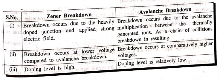
Zener Breakdown
(i) Breakdown occurs
due to the heavily doped junction and applied strong electric field.
(ii) Breakdown occurs
at lower voltage compared to avalanche breakdown.
(iii) Doping level is
high.
Avalanche Breakdown
(i) Breakdown occurs
due to the avalanche multiplication between the thermally generated ions. As a
chain of collisions breakdown in resulting.
(ii) Breakdown occurs
at comparatively higher voltages.
(iii) Doping level is
relatively low.
8.
Define the terms knee voltage and breakdown voltage with respect to diodes.
Knee
voltage: It is the forward voltage of a PN diode at which
the current through the junction starts increasing rapidly.
Breakdown
voltage: It is the reverse voltage of a PN junction diode at
which the junction breaks down with sudden rise in the reverse current.
9.
Define peak inverse voltage. (PIV)
Peak inverse voltage is
the maximum reverse voltage that can be applied to the PN junction without
damage to the junction. If the reverse voltage across the junction exceeds to
its peak inverse voltage, the junction may be destroyed due to excessive heat.
10.
Define and explain maximum forward current.
Maximum forward current
is the highest instantaneous forward current that a PN junction can conduct
without damage to the junction. If the forward current in a PN junction is more
than this rating, the junction will be damaged due to overheating.
11.
Explain the following with reference to a PN diode: Forward resistance, Reverse
resistance and cut in voltage.
Forward resistance
The resistance offered
by a diode to forward bias is known as forward resistance.
Reverse resistance
The resistance offered
by the diode to the reverse bias is known as reverse resistance. The reverse
resistance is very high compared to the forward resistance. In germanium diodes
the ratio of reverse to forward resistance is 4 × 10⁴ : 1 whereas
for the silicon diode the ratio is 1× 10⁶:1
Cut in voltage:
This is the voltage at which the forward bias curve abruptly increase from the
smaller value. The cut in voltage of germanium is 0.3 V and for silicon it is
0.6 V.
12.
Explain diode forward and reverse recovery times.
If the external voltage
is suddenly reversed in a diode circuit which has been carrying current in the
forward direction, the diode current will not immediately fall to its steady‒state
reverse voltage value. Until such time as the injected or excess minority‒carrier
has dropped nominally to zero, the diode will conduct easily. This time is
known as diode reverse Recovery time. Similarly diode forward recovery time
corresponds to sudden reversal of external voltage in the reverse direction.
13.
A 5V battery is connected across the two diodes connected in series opposing.
Find the voltage drop across each diode at room temperature.
At the two diodes are
connected in opposite direction, one of the diode will be reverse biased.
Therefore no current will flow in the circuit hence no voltage drop will be
there.
14.
What is avalanche multiplication in PN junction diode?
Consider a thermally
generated carrier which has acquired kinetic energy from the applied voltage.
Now the carrier is moving fastly with high kinetic energy. During its travel it
is colliding with some other ions hence causing the rupture in covalent bonds.
Therefore, one carrier may generated number of carrier by collisions. The newly
generate carriers may also acquire enough energy from the applied field. They
can collide with crystal ions and generate new electrons pairs. This process is
continuous and cumulative. It is known as avalanche multiplication.
15.
What is junction capacitance?
Any variation of the
charge within a P‒n diode with an applied voltage variation yields a
capacitance. This capacitance related to the depletion layer charge in a p‒n
diode is called the junction capacitance.
16.
What is ideal diode? Draw its V‒I characteristics.
An ideal diode is a
diode which has,
(i) No forward
resistance i.e., Rf=0.
(ii) Therefore no
voltage drop across it i.e., vf =
0. It acts as a conductor.
(iii) Under reverse
bias, Resistance is infinite. It acts as a open circuit.

In simple terms, an
ideal diode allows current to flow in the forward direction without any
resistance and completely prevent the flow of current in reverse direction.
17.
Define power dissipation of a zener diode.
It is the product of
reverse recovery current & the reverse voltage.
Power dissipation =
(reverse recover current) × (reverse voltage)
18.
Mention the advantages and disadvantages of zener diode.
advantages
(i) It is a heavily
doped diode
(ii) Depletion layer
will be thin
(ii) Consequently
breakdown occurs at lower reverse voltage
(iv) Zener diode is
operated at reverse biased condition
(v) It can be operated
as a voltage regulator
(vi) Size is small
& less space is occupied
(vii) Operation is
speed
Disadvantages
(i) Limited power rating
(ii) The operation of
the diode is temperature sensitive
19.
How does a PN junction diode behave under forward and reverse biased condition?
A PN junction diode
will behave as, closed switch under forward bias, and, open switch under
reverse bias conditions.
20.
Sketch the VI characteristics of a PN junction diode and mark various
operations.

21.
What are majority and minority carriers in a semiconductor?
P‒type Semiconductor
Holes are the majority
carriers and electrons are minority carriers.
n‒type Semiconductor
Electrons are majority
carriers and holes are minority carriers.
For a particular
semiconductors, the larger number of charge carriers is called to be majority
carriers and the smaller number of charge carrier is called to be minority
carriers.
22.
Define drift current and diffusion current?
Drift current:
It is defined as the flow of electric current due to the motion of the charge
carriers under the influence of an external electric field.
Diffusion current:
In a semiconductor, the charge carriers have the tendency to move from the
region of higher concentration to the region of lower concentration, of the
same type of charge carriers. Thus the movement of charge carriers takes place
which results in a current called diffusion current.
23.
Write the difference between the PN junction diode and Zener diode?
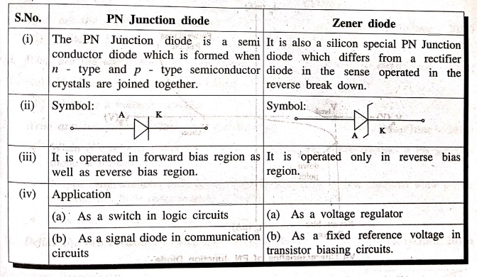
PN Junction diode
(i) The PN Junction
diode is a semi conductor diode which is formed when n type and p type
semiconductor crystals are joined together.
(iii) It is operated in
forward bias region as well as reverse bias region.
(iv) Application (a) As
a switch in logic circuits (b) As a signal diode in communication circuits.
Zener diode
(i) It is also a
silicon special PN Junction diode which differs from a rectifier diode in the
sense operated in the reverse break down.
(iii) It is operated
only in reverse bias region.
(iv) Application (a) As
a voltage regulator (b) As a fixed reference voltage in transistor biasing
circuits.
24.
Write any two salient points on a p‒n junction.
• It is lightly doped
diode
• During reverse biased
condition, Avalanche breakdown occurs.
• Used only in forward
bias condition as switch for rectifier circuits.
25.
What is meant by Zener effect?
Zener
effect
The zener breakdown
mechanism is fundamentally different from avalanche breakdown. Zener breakdown
occurs when the electric field in the deflection layer increases to the point where
it can break covalent bonds and generate electron‒hole pairs. The electrons
generated in this way will be swept by the electric field into N‒side and holes
into P‒sides. Thus, these electrons and holes constitute reverse current across
the junction that helps to supports the external current. In terms of an energy
band structure, in this breakdown process an electron makes a transition from
the valance band to the conduction band without the interaction of any other
particle. Once the Zener effect starts a large number of carriers can be
generated with a negligible increase in the junction voltage. In fact the zener
process is quantum tunnelling. However, later on the breakdown in junction
which may result from avalanche multiplication or tunneling was in general
called Zener breakdown.
The maximum reverse
bias potential that can be applied before entering the zener region is called
the peak inverse voltage or peak voltage.
26.
Why is zener diode used as a voltage regulator?

From the VI
characteristics we can see that, zener diode has a constant negative voltage regardless
of the value of current flowing through the diode and remains nearly constant
even with large change in current. This ability to control it's voltage can be
used to regulate or stabilise a voltage source against supply or load
variations.
27.
What are the other names of Zener diode?
• Backward diode
• Transient voltage
suppression diode
• Voltage regulator
28.
Define breakdown voltage.
The breakdown voltage
of a diode is the minimum reverse voltage to make the diode conduct in reverse.

29.
What are the applications of diode?
(i) Switches
(ii) Rectifiers
30.
What are the applications of zener diode?
(a) Used as a constant
voltage source
(b) Used as a voltage
regulator
31.
Write any two salient points on a p‒n junction.
When N‒type and p‒type
semiconductor crystals are joined together a PN junction diode is formed.
N‒type semiconductor
material has high concentration of free electrons while p‒type material has
high concentration of holes.
It is used as a
switches and rectifiers.
32.
Define the two breakdown conditions in zener diode.
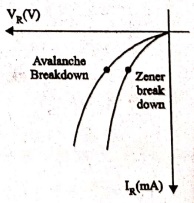
Avalanche Breakdown
As the applied reverse
bias voltage increases, the field across the junction increases corresponding, then
the Avalanche breakdown occurs at comparatively higher breakdown voltage.
Zener Breakdown
When the reverse bias
field across the junction is sufficiently high, then the zener breakdown occurs
at comparatively lower breakdown voltage.
33.
Draw the characteristics of zener diode.

34.
Draw the circuit diagram of half wave rectifier.

Basic Electronics and Electrical Engineering: Chapter 1: Basic Electronics : Tag: Basic Engineering : - Basic Electronics: 2 Marks Important Questions with Answers
Basic Electronics and Electrical Engineering: Chapter 1: Basic Electronics
Under Subject

Basic Electronics and Electrical Engineering
EE25C04 1st Semester ECE Dept | 2025 Regulation | 2nd Semester 2025 Regulation
Related Subjects

English Essentials I
EN25C01 1st Semester | 2025 Regulation | 1st Semester 2025 Regulation

தமிழர் மரபு - Heritage of Tamils
UC25H01 1st Semester | 2025 Regulation | 1st Semester 2025 Regulation
Applied Calculus
MA25C01 Maths 1 M1 - 1st Semester | 2025 Regulation | 1st Semester 2025 Regulation
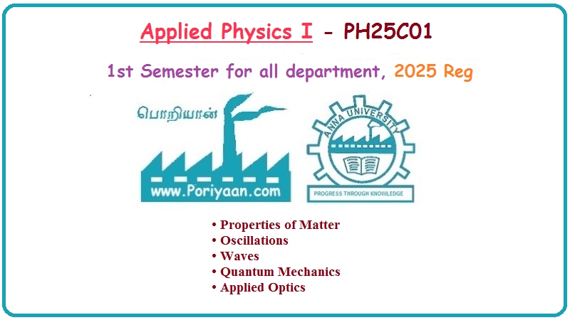
Applied Physics I
PH25C01 1st Semester | 2025 Regulation | 1st Semester 2025 Regulation

Applied Chemistry I
CY25C01 1st Semester | 2025 Regulation | 1st Semester 2025 Regulation

Makerspace
ME25C04 1st Semester | 2025 Regulation | 1st Semester 2025 Regulation

Computer Programming C
CS25C01 1st Semester | 2025 Regulation | 1st Semester 2025 Regulation

Computer Programming Python
CS25C02 1st Semester | 2025 Regulation | 1st Semester 2025 Regulation
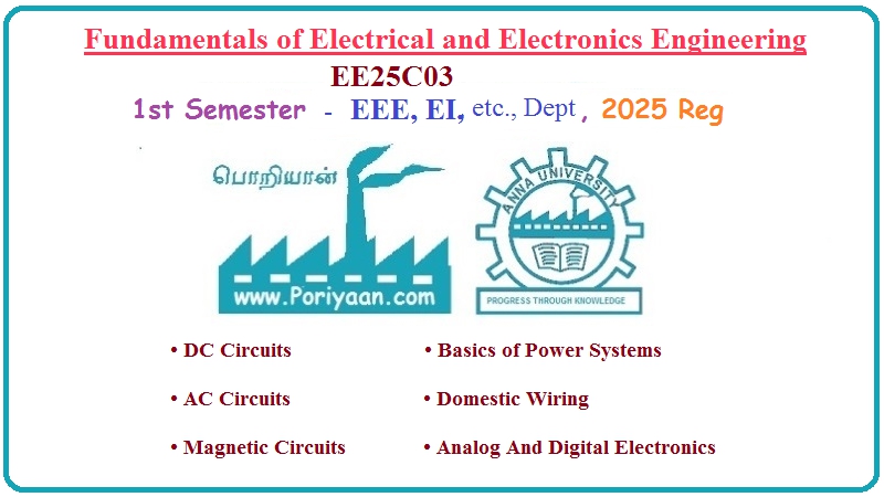
Fundamentals of Electrical and Electronics Engineering
EE25C03 1st Semester | 2025 Regulation | 1st Semester 2025 Regulation
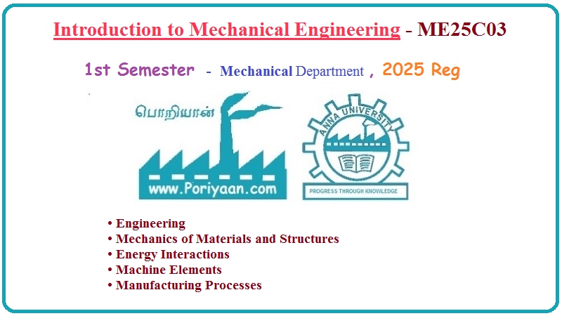
Introduction to Mechanical Engineering
ME25C03 1st Semester | 2025 Regulation | 1st Semester 2025 Regulation

Introduction to Civil Engineering
CE25C01 1st Semester Civil Department | 2025 Regulation | 1st Semester 2025 Regulation

Essentials of Computing
CS25C03 1st Semester - AID CSE IT Department | 2025 Regulation | 1st Semester 2025 Regulation

Applied Physics I Laboratory
PH25C01 1st Semester practical Laboratory Manual | 2025 Regulation | 1st Semester Laboratory 2025 Regulation

Applied Chemistry I Laboratory
CY25C01 1st Semester practical Laboratory Manual | 2025 Regulation | 1st Semester Laboratory 2025 Regulation

Computer Programming C Laboratory
CS25C01 1st Semester practical Laboratory Manual | 2025 Regulation | 1st Semester Laboratory 2025 Regulation

Computer Programming Python Laboratory
CS25C02 1st Semester practical Laboratory Manual | 2025 Regulation | 1st Semester Laboratory 2025 Regulation
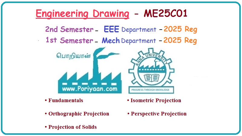
Engineering Drawing
ME25C01 EEE Mech Dept | 2025 Regulation | 2nd Semester 2025 Regulation
Basic Electronics and Electrical Engineering
EE25C04 1st Semester ECE Dept | 2025 Regulation | 2nd Semester 2025 Regulation