Basic Electronics and Electrical Engineering: Chapter 1: Basic Electronics
PN Junction Diode
Symbol, Operation, VI characteristic, Effect on capacitance
1. Diode Under Forward Bias Condition, 2. Diode Under Reverse Bias Condition, 3. Effect on capacitance of a PN junction diode
PN
JUNCTION DIODE
A PN Junction diode or
semiconductor diode is formed when n‒type and p‒type semiconductor crystals are
joined together. However mechanically joining two pieces of semiconductor
creates all sorts of problems structurally, electrically and chemically at the
interface, making it unsuitable for device application.
In practice, adding
acceptor impurities to an wafer or donor to a p‒type wafer forms a p‒n
junction.
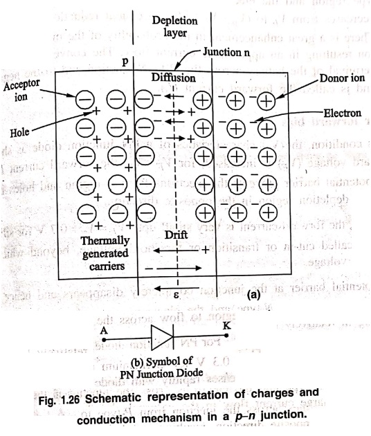
As shows in fig 1.26,
the N‒type material has high concentration of free electrons while P‒type
material has high concentration of holes. Therefore at the junction there is a
tendency for free electrons to diffuse over the P‒side and holes to N‒side. This
process is called diffusion. Electrons coming into P‒material combine with the
holes of the acceptor atoms and creating a negatively charged layer of
unneutralized acceptor ions fixed in space. Similarly the holes moving into the
N‒material combine with free electrons of the donor atoms and a positively
charged layer of unneutralised donor ions is formed in the N‒side near the
junction. Thus the narrow width of fixed positive charges on the n‒side of the
junction and fixed negative charges on the p‒side of the junction appear as
shown in fig 1.26. This region is known as the depletion region (or space
charge region or transition region). It creates a built‒in‒potential or barrier
potential vb across the junction. The barrier potential vb
is 0.3 V for germanium and 0.7 V for silicon.
Diode Under Forward Bias Condition
A forward bias of PN
Junction diode is established by applying positive potential of a battery
(voltage v) to P‒side and its negative is connected to N‒side, as shown in fig
1.27.

Operation
Under the forward bias
condition the applied positive potential repels the holes in P‒type region so
that the hole move towards the junction and the applied negative potential
repels the electrons in the N‒type region and the electrons move towards the
junction. Hence the effective barrier height decreases from Vb to (Vb‒V)
with consequent reduction in the width of the depletion region. There is a
great enhancement in the probability of the majority carriers moving across the
junction resulting in an appreciable current flow. The conventional current
flows from the positive terminal of the battery across the P to N‒junction and
to the negative terminal of the battery and is called the forward current (If).
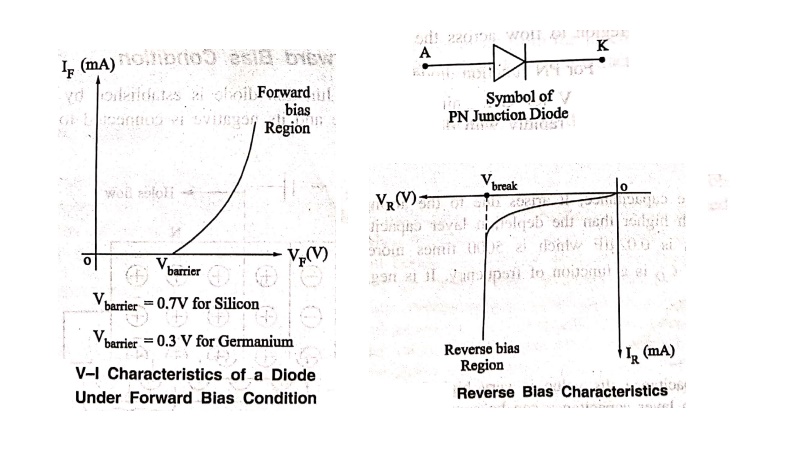
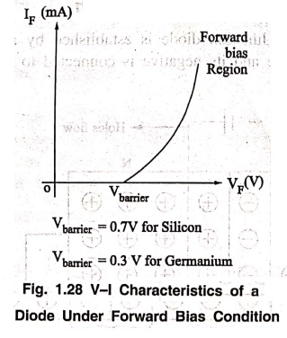
V‒I characteristic under forward bias
Under forward bias
condition, the V‒I characteristics of a PN Junction diode as shown in fig.
1.28. As the forward voltage (VF) is increased, for VF<
Vb, the forward current IF is almost zero because the
potential barrier prevents the electrons from N‒region and holes from P‒region
to flow across the depletion region in the opposite direction.
For PN Junction diode,
the forward current is very small upto VF=Vγ=0.7 V for
silicon and 0.3 V for Germanium called cut‒in or transition or threshold
voltage, beyond which it increases rapidly with diode voltage.
For VF> Vb,
the potential barrier at the junction completely disappears and hence the holes
across the junction from P‒type to N‒type and the electrons cross the junction
in the opposite direction, resulting in relatively large current flow in the
external circuit.
Diode Under Reverse Bias Condition
If an external voltage
is applied to P‒N junction such that positive terminal of the battery is
connected to N‒type region and the negative terminal of battery is connected to
the P‒type region, a reverse bias condition is established.
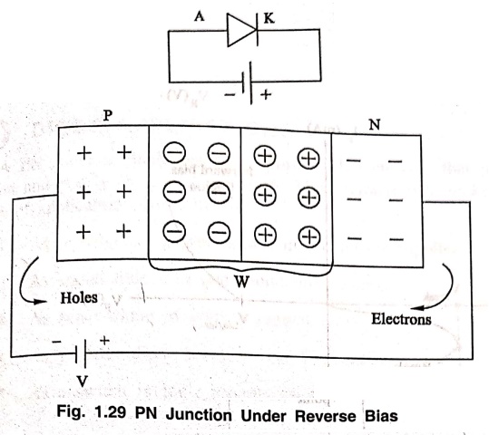
Operation
Under reverse bias
condition, the majority electrons which move away from the junction are
attracted by the positive potential at the N‒side and similarly the majority
holes are attracted towards the negative polarity of the battery connected to
the P‒side.
As a result, the number
of uncovered positive ions in the depletion region of the N‒type material and
uncovered negative ions in the P‒type material will increase. The net‒effect is
widening of the depletion region and the barrier potential rises. The majority
carriers cannot overcome this barrier energy and their flow is reduced to zero.
The minority carriers however will cross the junction at reverse bias voltage
and contribute to reverse current. The minority carrier current reaches its
saturation value at even very low reverse bias voltage because of the low
concentration of minority carriers. The current that exists under reverse‒bias
condition is called the reverse saturation current. The magnitude of reverse
saturation current mainly depends upon junction temperature because the major
source of minority carriers is thermally broken covalent bonds.
VI Characteristic under Reverse Bias
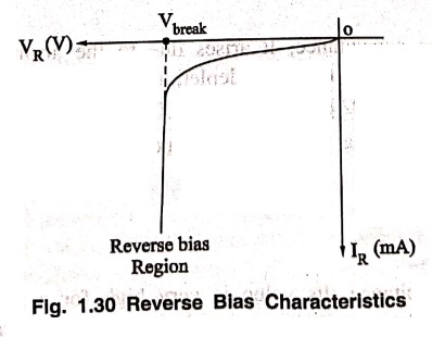
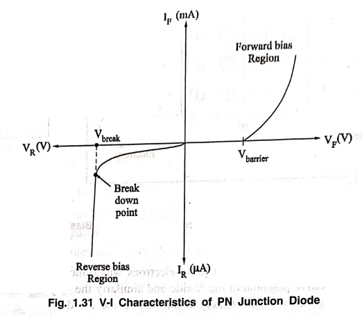
For large applied
revere bias voltage, the free electrons from the N‒type region moving towards
the positive terminal of the battery acquire sufficient energy to mover with
high velocity to dislodge valence electrons from semiconductor atoms in the
crystal. These newly liberated electrons, in turn acquires sufficient energy to
dislodge other parent electrons. Thus a large number of free electrons are
formed which is called as an avalanche of free electrons. This leads to the
breakdown of the junction leading to very large reverse current. The reverse
voltage at which the junction breakdown occurs is known as breakdown voltage.
Effect on capacitance of a PN junction diode
Forward Biased
Diffusion or storage
capacitance, It arises due to the arrangement of minority carrier density. Its
value is much higher than the depletion layer capacitance. The typical value of
diffusion capacitance CD is 0.02 μF which is 5000 times more than
the depletion layer capacitance. The value of CD is a function of
frequency. It is negligible for a reverse biased PN junction.
Reverse Biased
Depletion layer
capacitance. Its is value is very high for a reverse biased PN junction. The
value of CT depletion layer capacitance can be controlled by varying
the applied reverse
voltage, because CT depends upon the nature of a PN junction.
Basic Electronics and Electrical Engineering: Chapter 1: Basic Electronics : Tag: Basic Engineering : Symbol, Operation, VI characteristic, Effect on capacitance - PN Junction Diode
Basic Electronics and Electrical Engineering: Chapter 1: Basic Electronics
Under Subject

Basic Electronics and Electrical Engineering
EE25C04 1st Semester ECE Dept | 2025 Regulation | 2nd Semester 2025 Regulation
Related Subjects

English Essentials I
EN25C01 1st Semester | 2025 Regulation | 1st Semester 2025 Regulation

தமிழர் மரபு - Heritage of Tamils
UC25H01 1st Semester | 2025 Regulation | 1st Semester 2025 Regulation

Applied Calculus
MA25C01 Maths 1 M1 - 1st Semester | 2025 Regulation | 1st Semester 2025 Regulation

Applied Physics I
PH25C01 1st Semester | 2025 Regulation | 1st Semester 2025 Regulation

Applied Chemistry I
CY25C01 1st Semester | 2025 Regulation | 1st Semester 2025 Regulation

Makerspace
ME25C04 1st Semester | 2025 Regulation | 1st Semester 2025 Regulation

Computer Programming C
CS25C01 1st Semester | 2025 Regulation | 1st Semester 2025 Regulation

Computer Programming Python
CS25C02 1st Semester | 2025 Regulation | 1st Semester 2025 Regulation
Fundamentals of Electrical and Electronics Engineering
EE25C03 1st Semester | 2025 Regulation | 1st Semester 2025 Regulation

Introduction to Mechanical Engineering
ME25C03 1st Semester | 2025 Regulation | 1st Semester 2025 Regulation

Introduction to Civil Engineering
CE25C01 1st Semester Civil Department | 2025 Regulation | 1st Semester 2025 Regulation

Essentials of Computing
CS25C03 1st Semester - AID CSE IT Department | 2025 Regulation | 1st Semester 2025 Regulation

Applied Physics I Laboratory
PH25C01 1st Semester practical Laboratory Manual | 2025 Regulation | 1st Semester Laboratory 2025 Regulation

Applied Chemistry I Laboratory
CY25C01 1st Semester practical Laboratory Manual | 2025 Regulation | 1st Semester Laboratory 2025 Regulation

Computer Programming C Laboratory
CS25C01 1st Semester practical Laboratory Manual | 2025 Regulation | 1st Semester Laboratory 2025 Regulation

Computer Programming Python Laboratory
CS25C02 1st Semester practical Laboratory Manual | 2025 Regulation | 1st Semester Laboratory 2025 Regulation

Engineering Drawing
ME25C01 EEE Mech Dept | 2025 Regulation | 2nd Semester 2025 Regulation
Basic Electronics and Electrical Engineering
EE25C04 1st Semester ECE Dept | 2025 Regulation | 2nd Semester 2025 Regulation