Basic Electronics and Electrical Engineering: Chapter 1: Basic Electronics
Zener Diode
Reverse Characteristic, Applications, Difference
1. Reverse Characteristic of a Zener Diode 2. Applications of Zener diode 3. Difference between the PN junction diode and zener diode 4. Applications of Zener diode as voltage regulator
ZENER
DIODE
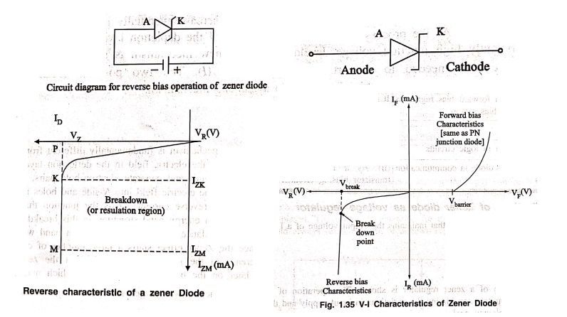
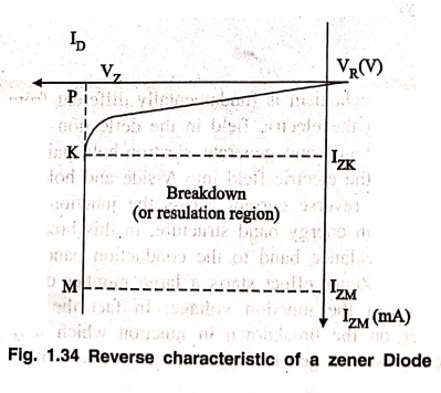
A zener diode is also
called as voltage reference, voltage regulator or breakdown diode Fig (1.33)
shows a schematic symbol for a zener diode.
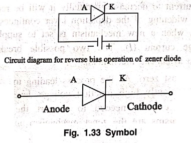
The zener diode is a silicon PN junction device which differs from a rectifier diode, in the sense that it is operated in the reverse breakdown region. The breakdown voltage of a zener diode is set by carefully controlling the doping level during manufacture.
Reverse Characteristic of a Zener Diode
We have just discussed
that a zener diode is operated only in the reverse‒bias region. That is why we
shall discuss its characteristic in this region only. Fig (1.34) shows the
reverse portion of the V‒I characteristic of the zener diode.
It may be noted from
this figure that as the reverse voltage (VR) is increased, the
reverse current (Iz ‒ zener current) remains negligibly small upto
the 'knee' of the curve (point ‘p'). At this point, the effect of breakdown
process begins. From the bottom of the knee, the breakdown voltage (vz)
remains essentially constant. This ability of a diode is called regulating
ability. It maintains an essentially a constant voltage across its terminals
over a specified range of zener current values. The following two points are
important from the characteristic of a zener diode.
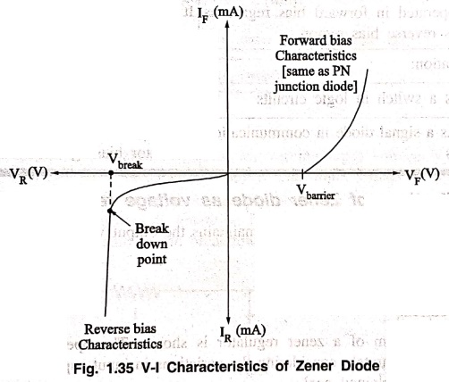
(i) There is a minimum
value of zener current called breakover current designed as Iz(min)
which must be maintained in order to keep the diode in breakdown (or
regulation) region. When the current is reduced below the knee of the curve the
voltage changes drastically and the regulation is lost.
(ii) There is a maximum
value of zener current designated as Iz(max) above which the diode
may be damaged.
Applications of Zener diode
• As voltage
regulators.
• As fixed reference
voltage in power supplies and transistor biasing.
• As clippers in wave‒shaping
circuits.
Difference between the PN junction diode and zener diode.
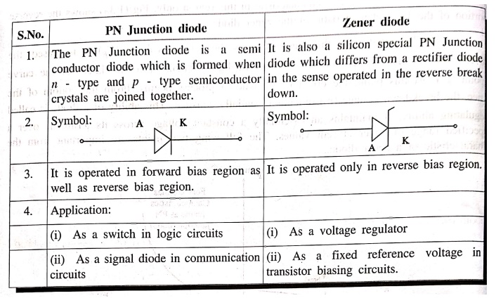
PN Junction diode
• The PN Junction diode
is a semi conductor diode which is formed when n-type and p-type semiconductor crystals
are joined together.
• It is operated in
forward bias region as well as reverse bias region.
• Application: (i) As a
switch in logic circuits (ii) As a signal diode in communication circuits
Zener diode
• It is also a silicon
special PN Junction diode which differs from a rectifier diode in the sense
operated in the reverse break down.
• It is operated only
in reverse bias region.
• Application: (i) As a
voltage regulator (ii) As a fixed reference voltage in transistor biasing circuits.
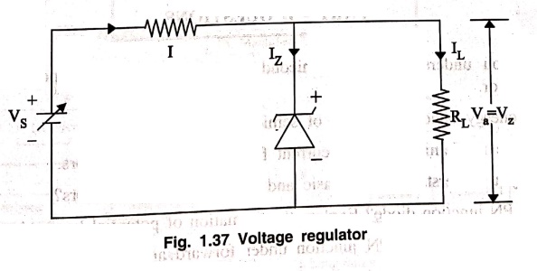
Applications of Zener diode as voltage regulator
A voltage regulator is
a circuit that maintains the output voltage of a DC power supply constant
against variations in
• Input AC voltage
• Load current
The circuit diagram of
a zener regulator is shown. The operation of zener regulator can be explained
by separately considering the variations in input supply and the load current.
These two cases are explained next.

Zener regulator with
varying voltage regulator/
(i) If RL Increases
IL decreases, to keep constant. Iz increases,
RL ↑ → IL (min) ↓ → Iz
(max) ↑
IL (min) = I ‒ IL (max) ... (1)
(ii) If RL
decreases IL increases, to keep I constant Iz decreases,
RL ↓ → IL (max) ↑ → Iz
(min) ↓
IL (max) = I − Iz (min) ….(2)
(iii) The maximum power
dissipation in zener remains same as
PD=VzIz (max) ….(3)
Regulation with Varying input voltage
The circuit diagram of
a zener regulator for varying input voltage is illustrated. The input voltage Vs
is shown as a variable DC supply. This input voltage is unregulated, as it
varies due to the variations in the input AC supply of the rectifier. In Fig.
1.37, the zener diode is reverse biased. The necessary condition for the
operation of this circuit is that the zener diode should always remain in the
breakdown region. Throughout the operation of the circuit.
Zener regulator with
varying input voltage
It can be seen that the
output is
Vo = Vz
is constant.
VL = Vo
/ RL = Vz / RL = constant
I = 1L+ IZ
Now if Vo
increases then the total current I increases, But IL is constant as
Vz is constant. Hence the current Iz increases to keep IL
constant.
If Vo
decreases then current I decreases. But to keep IL constant, Iz
decreases.
Regulation Varying with load
The circuit conditions
for the zener regulator with varying load current is illustrated in fig. The
load current IL, will vary if the load resistor, RL is
variable. The load current increases when the load resistance decreases, and
the load current decreases if the load resistance increases.
The input voltage is
constant while the load resistance RL is variable. As VS
is constant and Vo=Vz is constant, then for constant R the current I is
constant.
I
= [ Vin ‒ VZ ] / R
Basic Electronics and Electrical Engineering: Chapter 1: Basic Electronics : Tag: Basic Engineering : Reverse Characteristic, Applications, Difference - Zener Diode
Basic Electronics and Electrical Engineering: Chapter 1: Basic Electronics
Under Subject

Basic Electronics and Electrical Engineering
EE25C04 1st Semester ECE Dept | 2025 Regulation | 2nd Semester 2025 Regulation
Related Subjects

English Essentials I
EN25C01 1st Semester | 2025 Regulation | 1st Semester 2025 Regulation

தமிழர் மரபு - Heritage of Tamils
UC25H01 1st Semester | 2025 Regulation | 1st Semester 2025 Regulation

Applied Calculus
MA25C01 Maths 1 M1 - 1st Semester | 2025 Regulation | 1st Semester 2025 Regulation

Applied Physics I
PH25C01 1st Semester | 2025 Regulation | 1st Semester 2025 Regulation

Applied Chemistry I
CY25C01 1st Semester | 2025 Regulation | 1st Semester 2025 Regulation

Makerspace
ME25C04 1st Semester | 2025 Regulation | 1st Semester 2025 Regulation

Computer Programming C
CS25C01 1st Semester | 2025 Regulation | 1st Semester 2025 Regulation

Computer Programming Python
CS25C02 1st Semester | 2025 Regulation | 1st Semester 2025 Regulation
Fundamentals of Electrical and Electronics Engineering
EE25C03 1st Semester | 2025 Regulation | 1st Semester 2025 Regulation
Introduction to Mechanical Engineering
ME25C03 1st Semester | 2025 Regulation | 1st Semester 2025 Regulation

Introduction to Civil Engineering
CE25C01 1st Semester Civil Department | 2025 Regulation | 1st Semester 2025 Regulation

Essentials of Computing
CS25C03 1st Semester - AID CSE IT Department | 2025 Regulation | 1st Semester 2025 Regulation

Applied Physics I Laboratory
PH25C01 1st Semester practical Laboratory Manual | 2025 Regulation | 1st Semester Laboratory 2025 Regulation

Applied Chemistry I Laboratory
CY25C01 1st Semester practical Laboratory Manual | 2025 Regulation | 1st Semester Laboratory 2025 Regulation

Computer Programming C Laboratory
CS25C01 1st Semester practical Laboratory Manual | 2025 Regulation | 1st Semester Laboratory 2025 Regulation

Computer Programming Python Laboratory
CS25C02 1st Semester practical Laboratory Manual | 2025 Regulation | 1st Semester Laboratory 2025 Regulation
Engineering Drawing
ME25C01 EEE Mech Dept | 2025 Regulation | 2nd Semester 2025 Regulation
Basic Electronics and Electrical Engineering
EE25C04 1st Semester ECE Dept | 2025 Regulation | 2nd Semester 2025 Regulation