Computer Organization and Architecture: Chapter 2: Arithmetic for Computers
Carry Look ahead Adder
Questions: 1. Explain in detail the principle of carry‒look‒ahead adder. 2. What is the disadvantages in using a ripple carry adder? 3. Explain the design of a 4‒bit carry‒look ahead adder. 4. In carry‒look ahead addition, explain generate stage Gi and propagate Pi functions for stage i with the help of boolean expression for Gi and Pi.
Carry Look‒ahead
Adder
•
The n‒bit adder ripple carry adder discussed in the last section is implemented
using full‒adder stages. In which the carry output of each full‒adder stage is
connected to the carry input of the next higher‒order stage. Therefore, the sum
and carry outputs of any stage cannot be produced until the input carry occurs;
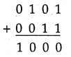
this leads to a time delay in the addition process. This delay is known as carry propagation delay, which can be
best explained by considering the following addition.
•
Addition of the LSB position produces a carry into the second position. This
carry, when added to the bits of the second position (stage), produces a carry
into the third position. The latter carry, when added to the bits of the third
position, produces a ad carry into the last position. The key thing to notice
in this example is that the sum gibs bit generated in the last position (MSB)
depends on the carry that was generated by as be the addition in the previous
positions. This means that, adder will not produce correct result until LSB
carry has propagated through the intermediate full‒adders. This represents a
time delay that depends on the propagation delay produced in each full‒adder.
For example, if each full‒adder is considered to have a propagation delay of 30
ns, then S3 will not reach its correct value until 90 ns after LSB
carry is generated. Therefore, total time required to perform addition is
90+30= 120 ns.
• Obviously, this situation becomes much worse
if we extend the adder circuit to add a greater number of bits. If the adder
were handling 16‒bit numbers, the carry propagation delay could be 480 ns.
•
Generally, carry propagation delay and sum propagation delay are measured in
terms of gate delays. Looking at Fig. 2.1.9 we can notice that for full‒adder Cout
requires two gate delays and sum requires only one gate delay. When we connect
such full adder circuits in cascade to generate n‒bit ripple adder as shown in
Fig. 2.1.11, Cn‒1 is available in 2(n‒1) gate delays, and Sn‒1 is
correct one XOR gate delay later. The final carry‒out, Cn is available
after 2n gate delays. Thus for 4‒bit ripple adder C4 is available
after 8(2×4) gate delays, C3 is available in 6[2(4‒1)] gate delays
and S3 is available in 7 gate delays.
•
One method of speeding up this process by eliminating inter stage carry delay
is called lookahead‒carry addition.
This method utilizes logic gates to look at the lower‒order bits of the augend
and addend to see if a higher‒order carry is to be generated. It uses two
functions: carry generate and carry propagate.
•
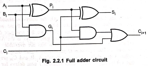
Consider the circuit of the full adder shown in Fig. 2.2.1. Here, we define two
to functions: Carry generate and carry
propagate.
Pi
= Ai  Bi
Bi
Gi = Ai
Bi
The
output sum and carry can be expressed as
Si
= Pi Ci
Ci
+1 Gi + Pi Ci
•
Gi is called a carry generate and it produces on carry when both Ai
and Bi are one, regardless of the input carry. Pi is
called a carry propagate because it is term associated with the propagation of
the carry from Ci to Ci+1. Now C i+1 can be
expressed as a sum of products function of the P and G outputs of all the
preceding stages. For example, the carriers in a four stage carry‒lookahead
adder are defined as troll follows:
C1
= G0 + P0Cin
C2
= G1 + P1C1 = G1+ P1Go
+ P1PoCin
C3
= G2 + P2C2 = G2 + P2G1+
P2P1Go+ P2P1PoCin
C4
= G3 + P3C3
= G3
+ P3G2 + P3P2G1 + P3P2P1Go
+ P3P2P1Po Cin
•
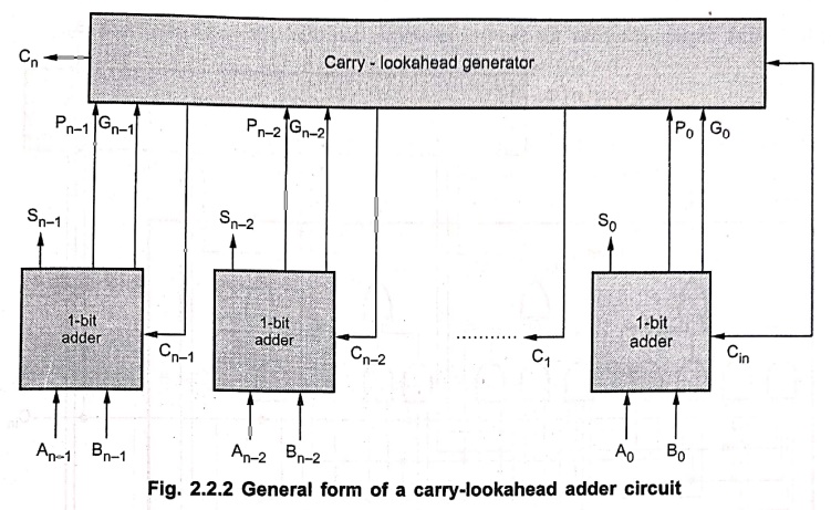
Fig. 2.2.2 shows the general form of a carry‒lookahead adder circuit designed
in this way.
•
We can further simplify the design by noting that the sum equation of stage i
Si
= Ai Bi Ci as Si =
Pi Gi Ci
•
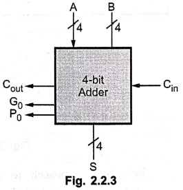
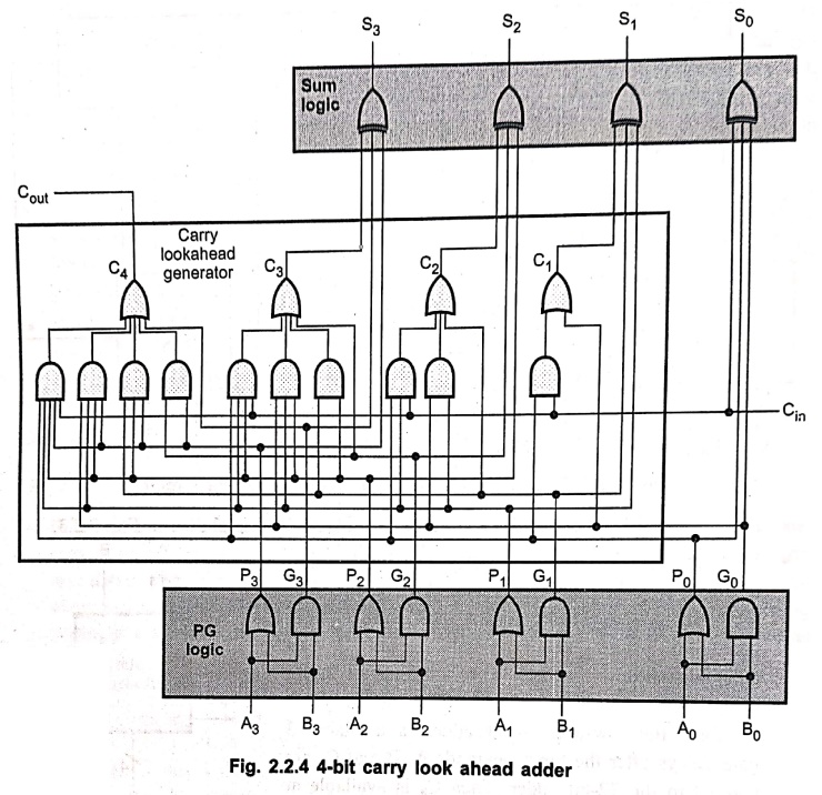
Combining equations for P and G, the carry‒lookahead equations, and the
modified sum equation, we obtain the 4‒bit carry‒lookahead adder as shown in
Fig. 2.2.3. Looking at Fig. 2.2.3 we can easily note that one gate delay is
needed to develop all Pi and Gi signals, followed by two
gate delays in the AND‒OR circuit for Ci+1. After a further XOR gate
delay, all sum bits are available. Therefore, independent of n, the n‒bit
addition process requires only 4 gate delays and all carries can be obtained
within 3 gate delays after the signals A, B and Cin are applied. In
comparison note that a 4‒bit ripple carry adder requires 7 gate delays for S3
and 8 gate delays for C4.
•
A complete 4‒bit carry‒lookahead adder in a block form is shown in Fig. 2.2.3.
•
We can cascade such 4‒bit carry‒lookahead adders to form a 16‒bit or 32‒bit
adder. We require four 4‒bit carry‒lookahead adders to form 16‒bit carry‒lookahead
adder and eight 4‒bit carry‒lookahead adders to form 32‒bit carry‒lookahead
adder. In 32‒bit adder, the carry out C4 form the low‒order 4‒bit
adder is available 3 gate delays after the input operands A, B and C0
are applied to the 32‒bit adder. Then C8 is available at the output
of the second adder after a further 2 gate delays, C12 is available
after a further 2 gate delays, and so on. Finally, C28 the carry‒in
to the high‒order 4‒bit adder, is available after a bold total of (6 × 2) + 3 =
15 gate delays, C32 is available after 2 more gate delays, i.e. after
17 gate delays and S31 is available after 3 gate delays, i.e. 18
gate delays. These gate delays are very less compared to total delays of 63 and
64 for S31 and C32 if ripple‒carry adder is used.
Multilevel generate and propagate functions
•
In the 32‒bit adder just discussed, the carriers C4, C8,
C12, ….. ripple through the 4‒bit adder blocks with two gate delays
per clock. This is analogous to the way that individual carries ripple through
each bit stage in a ripple‒carry adder.
By
using multi‒level block generate and propagate functions, it is possible to use
the lookahead approach to develop the carries C4, C8, C12,
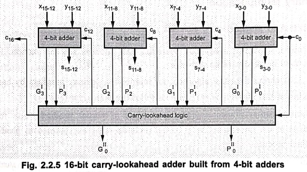
... in parallel, in a multi‒level carry‒lookahead circuit. Fig. 2.2.5 shows a
16‒bit adder implemented using four 4‒bit adder blocks. Here, blocks provide
new output functions defined as GIk and PIk
, where K = 0 for the first 4‒bit block, K = 1 for the second 4‒bit block
and so on. In the first block,
PI0
= P3P2P1P0
and
GI0
= G3 + P3G2 + P3P2G1
+ P3P2P1G0
•
Therefore, we can use first‒level GI and PI functions to
determine whether bit stage i generates or propagates a carry, and we can use
the second level GIK and PIK
functions to determine whether block K generates or propagates a carry. With
these new functions available, it is not necessary to wait for carries to
ripple through the 4‒bit blocks. Looking at Fig. 2.2.5, we can determine C16
as
C16
= GI3 + PI3GI2
+ PI3PI2GI1 +
PI3PI2PI1GI0
+ PI3PI2P1PI0C0
•
The above expression is identical in form to the expression for C4;
only variable names are different. Therefore, the structure of the carry‒lookahead
circuit in Fig. 2.2.5 is identical to the carry‒lookahead circuit shown in Fig.
2.2.4. However, it is important to note that the carries C4, C8,
C12 and C16 generated internally by the 4‒bit adder
blocks are not needed in Fig. 2.2.5 because they are generated by the multi‒level
carry‒lookahead circuits.
•
Let see the delay in producing outputs from the 16‒bit carry‒ahead adder. The
delay in developing the carries produced by the carry‒lookahead circuits is two
gate delays more than the delay needed to develop the GIK
and PIK functions. The GIK and PIK
functions require two gate delays and one gate delay, respectively, after the
generation of G i and
Pi. Therefore, all carries produced by the carry‒lookahead circuits
are available 5 gate delays after A, B and C0 are applied as inputs.
The carry C15 is generated inside the higher‒order 4‒bit block in
Fig. 2.2.5 in two gate delays after C12 followed by S15
in one further gate delay. Therefore, S15 is available after 8 gate
delays. These delays, 5 gate delays for C16 and 8 gate delays for S15
are less as compared to 9 and 10 gate delays for C16 and S15
in cascaded 4‒bit carry‒lookahead adder blocks, respectively.
•
We can cascade two 16‒bit adders to implement 32‒bit adder. Here, only two more
at gate delays are required to get C32 and S31 and C16
and S15, respectively. Therefore, C32 is available after
7 gate delays and S31 is available after 10 gate delays. These
delays are less compared to 18 and 17 gate delays for the same outputs if the
32‒bit adder is built from a cascade of eight 4‒bit adders.
•
If we go for third level then we can built 64‒bit using four 16‒bit adders.
Delay through this adder will be 12 gate delays for S63 and 7 gate
delays for C64.
Review Questions
1. Explain in detail
the principle of carry‒look‒ahead adder.
2. What is the
disadvantages in using a ripple carry adder?
3. Explain the design
of a 4‒bit carry‒look ahead adder.
4. In carry‒look ahead
addition, explain generate stage Gi and propagate Pi
functions for stage i with the help of boolean expression for Gi and
Pi.
Computer Organization and Architecture: Chapter 2: Arithmetic for Computers : Tag: Computer : - Carry Look ahead Adder
Computer Organization and Architecture: Chapter 2: Arithmetic for Computers
Under Subject
Computer Organization and Architecture
CW25201 3rd Semester IT department. | 2025 Regulation | 3rd Semester 2025 Regulation
Related Subjects
Discrete Mathematics
MA25C14 3rd Semester CSE,IT,CY,AIDS departments. | 2025 Regulation | 3rd Semester 2025 Regulation
Data Structures
CS25C08 3rd Semester CSE,IT,CY,AIDS departments. | 2025 Regulation | 3rd Semester 2025 Regulation
Computer Organization and Architecture
CW25201 3rd Semester IT department. | 2025 Regulation | 3rd Semester 2025 Regulation
Object Oriented Programming
CS25C07 3rd Semester IT department. | 2025 Regulation | 3rd Semester 2025 Regulation
Web Technologies
IT25301 3rd Semester IT department. | 2025 Regulation | 3rd Semester 2025 Regulation
English Communication Skills Laboratory I
EN25C03 3rd Semester all department. | 2025 Regulation | 3rd Semester 2025 Regulation
Skill Development Course I
3rd Semester all department. | 2025 Regulation | 3rd Semester 2025 Regulation