Computer Organization and Architecture: Chapter 2: Arithmetic for Computers
ALU Design
Arithmetic for Computers
Questions: 1. Explain the 4‒bit arithmetic circuit using the multiplexer. 2. Explain the 4‒bit arithmetic circuit with its function table. 3. Explain the design of the logic circuit using the multiplexer.
ALU
Design
1. Arithmetic Circuits
•
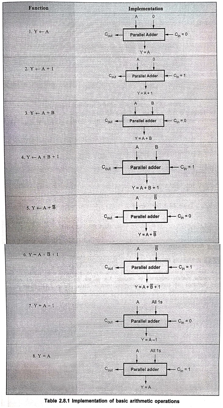
We have already seen how parallel adder can be constructed using number of full
adder circuits connected in cascade. Let us see the implementation of various
functions of arithmetic unit using parallel adder. Table 2.8.1 shows these
implementations.
•
Looking at Table 2.8.1 we can realize that by selecting proper B and Cin
inputs we can implement basic arithmetic operations. There are four possible B
inputs: true, complement, all 1s and all 0s and two possible Cin
inputs 0 and 1.
•
Referring Table 2.8.2, we can write truth table for B input with respect to So
and S1 signals as follows:
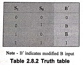
Note‒ B' indicates modified B input
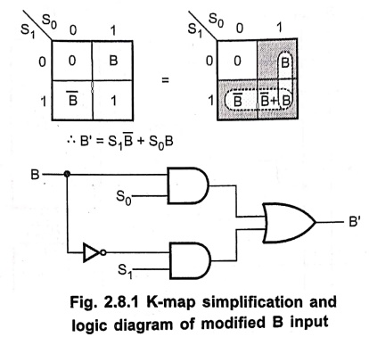
K‒map simplification
•
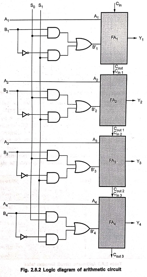
Using the logic diagram of modified B input we can draw the logic diagram of
arithmetic circuit, as shown in Fig. 2.8.2. (See Fig. 2.8.2 on next page).
•
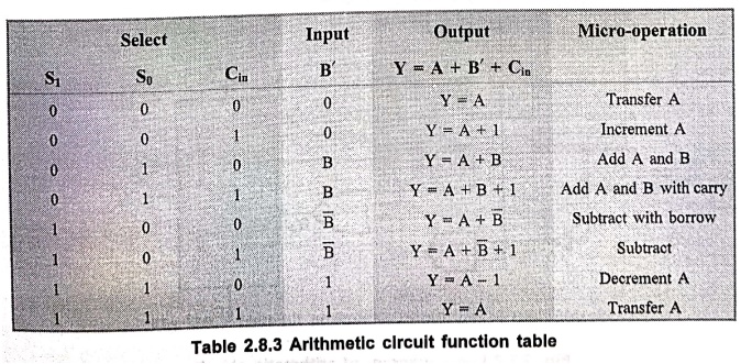
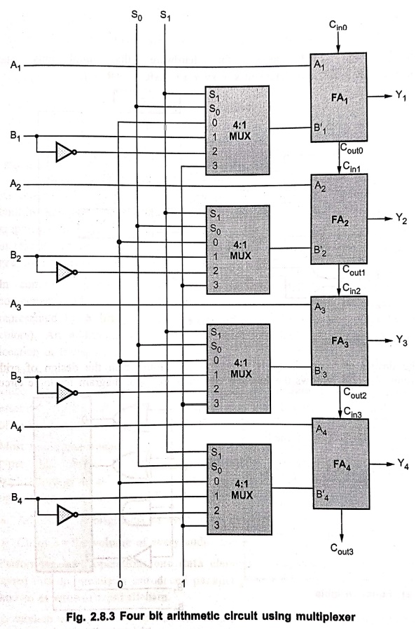
We can also implement the arithmetic circuit using multiplexers. Refer Table
2.8.4, we have four options for the B input of the full adder. We have to
select one of the four options according to select input S1 and S0.
We can implement a circuit for such requirement using 4:1 multiplexer. Fig.
2.8.3 shows the arithmetic circuit using multiplexers. (Refer Fig. 2.8.3 on
page 2‒79)
•
By controlling the value of B input of full adder with the two select inputs S1
and S0 and making Cin equal to 0 to 1, it is possible to
generate the eight arithmetic micro‒operations listed in Table 2.8.3.
Example: 1
Draw the block diagram
for the hardware that implements the following statements:
i) x + yz : AR←AR + BR
ii) x + xy + xz : AR←AR +1.
Solution:
i)
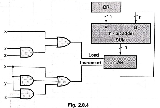
Fig. 2.8.4 shows the hardware that implements statement
x+yz:
AR← AR + BR and statement x + xy + xz: AR ← AR + 1.
2. Logic Circuits
•
The design of logic circuit is comparatively simple than the design of
arithmetic circuit. Fig. 2.8.5 shows the function table and the logic diagram
for logic circuit.
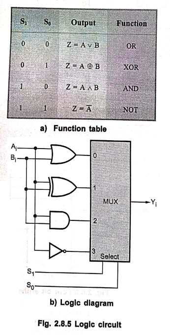
Note: The
logic diagram shown in Fig. 2.8.5 (b) is repeated n times for n‒bit logic
circuit. Therefore, inputs A and B, and output Y are shown with subscript i,
where i = 1, 2, ... n
Review Questions
1. Explain the 4‒bit
arithmetic circuit using the multiplexer.
2. Explain the 4‒bit
arithmetic circuit with its function table.
3. Explain the design
of the logic circuit using the multiplexer.
Computer Organization and Architecture: Chapter 2: Arithmetic for Computers : Tag: Computer : Arithmetic for Computers - ALU Design
Computer Organization and Architecture: Chapter 2: Arithmetic for Computers
Under Subject
Computer Organization and Architecture
CW25201 3rd Semester IT department. | 2025 Regulation | 3rd Semester 2025 Regulation
Related Subjects
Discrete Mathematics
MA25C14 3rd Semester CSE,IT,CY,AIDS departments. | 2025 Regulation | 3rd Semester 2025 Regulation
Data Structures
CS25C08 3rd Semester CSE,IT,CY,AIDS departments. | 2025 Regulation | 3rd Semester 2025 Regulation
Computer Organization and Architecture
CW25201 3rd Semester IT department. | 2025 Regulation | 3rd Semester 2025 Regulation
Object Oriented Programming
CS25C07 3rd Semester IT department. | 2025 Regulation | 3rd Semester 2025 Regulation
Web Technologies
IT25301 3rd Semester IT department. | 2025 Regulation | 3rd Semester 2025 Regulation
English Communication Skills Laboratory I
EN25C03 3rd Semester all department. | 2025 Regulation | 3rd Semester 2025 Regulation
Skill Development Course I
3rd Semester all department. | 2025 Regulation | 3rd Semester 2025 Regulation