Computer Organization and Architecture: Chapter 2: Arithmetic for Computers
Fast Multiplication
Arithmetic for Computers
Questions: 1. Explain the modified Booth's algorithm. 2. What is bit‒pair recoding? 3. Carry out bit pair recoding of following multipliers: 1 1 0 1 0, 0 1 1 0 1. 4. Design an array multiplier that multipliers two 4 bit numbers. Use AND gates and binary address. 5. Draw and explain 2‒bit by 2‒bit array multiplier. 6. Explain the concept of carry save addition for the multiplication operation, M × Q = P for 4‒bit operands, with diagram and suitable example. 7. Write a note on the carry‒save multiplier.
Fast Multiplication
•
There are two techniques for speeding up the multiplication process. In first
technique the maximum number of summands are reduced to n/2 for n‒bit operands.
•
The second technique, called the carry save addition reduces the time needed to
add the summand.
1. Bit‒Pair Recoding of Multipliers
•
To speed‒up the multiplication process in the Booth's algorithm a technique
called bit‒pair recoding is used. It is also called modified Booth's algorithm.
•
It halves the maximum number of summands.
•
In this technique, the Booth‒recoded multiplier bits are grouped in pairs. Then
each pair is represented by its equivalent single bit multiplier reducing total
number of multiplier bits to half.
•
For example pair (+ 1 ‒1) is equivalent to the pair (0 +1). That is, instead of
adding ‒1 times multiplicand at shifted position i to +1 times the multiplicand
at position i + 1, the same result is obtained by adding +1 times multiplicand
at position i. Similarly, (+1 0) is equivalent to (0 +2), (‒1 +1) is equivalent
to (0 ‒1) and so on.
•
By replacing pairs with their equivalents we can get bit‒pair recoded
multiplier.
•
But instead of deriving bit‒pair recoded multiplier from Booth recoded
multiplier one can directly derive it from original multiplier.
•
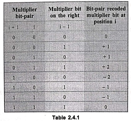
The bit‒pair recoding of multiplier can be directly derived from Table 2.4.1.
Table 2.4.1 shows the bit‒pair code for all possible multiplier bit options.
Example: 1
Find the bit‒pair code for
multiplier.
1 1 0 1 0.
Solution:
By referring table we can derive bit‒pair code as follows:

Example: 2
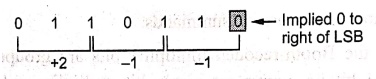
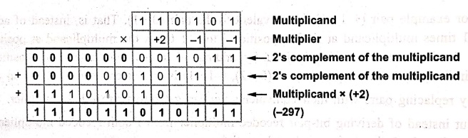
Multiply given signed 2's
complement numbers using bit‒pair recoding
A = 1 1 0 1 0 1 multiplicand (‒11)
B = 0 1 1 0 1 1 multiplier (+27)
Solution:
Let us find the bit‒pair code for multiplier.
Multiplication:
Example: 3
Give the Booth's recoding and bit‒pair
recoding of the number.
1 0 0 0 1 1 1 1 0 1 0 0 0 1 0 1
Solution:
Booth's recoding

Bit‒Pair recoding

Example: 4
Multiply the following pair of
signed 2's complement numbers using bit‒pair recoding of the multipliers: A = 010111,
B = 101100.
Solution :
A
= 0 10 1 1 1 Multiplicand (+23)
B
= 1 0 1 1 0 0 Multiplier (‒20)
Let
us find the bit‒pair code for multiplier
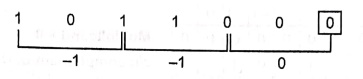
Multiplication
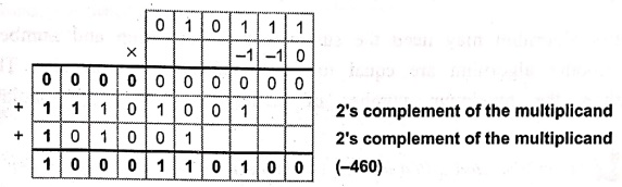
2's complement of the multiplicand
2's complement of the multiplicand
(‒460)
Example: 5
Explain Booth's algorithm to
multiply the following pair of signed two's complement numbers
A = 110011 multiplicand
B = 101100 multiplier
Also, implement the above using bit‒pair
Recoding and explain how it achieves faster multiplication
Solution :
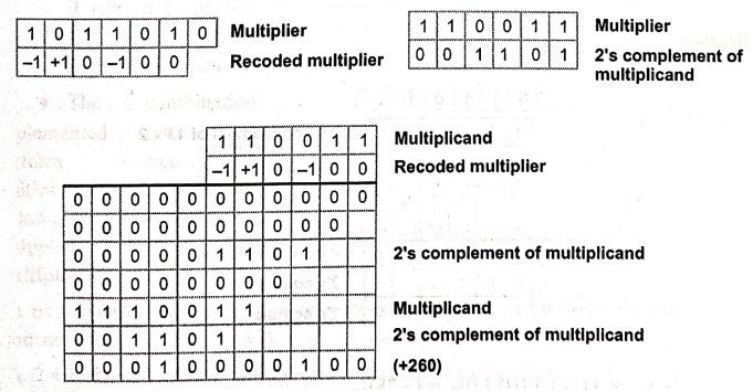
Implementation with bit‒pair
recoding
Bit‒pair
recoding for multiplier : ‒1 ‒1 0
Multiplication
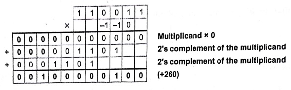
The
Booth's algorithm may need the summation at each step and number of steps
required in Booth's algorithm are equal to length of multiplier in bits. The
bit‒pair recoding halves the maximum number of summations. Hence it achieves
faster multiplication.
Example: 6
Show the multiplication of (+13)
and (‒6) using multiplier bit pair recoding technique.
Solution :
+ 13 = 0 1 1 0 1
‒ 6 =
1 0 1 0 2's complement of 6
Bit pair recoding of ‒ 6
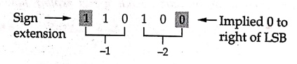
Multiplication
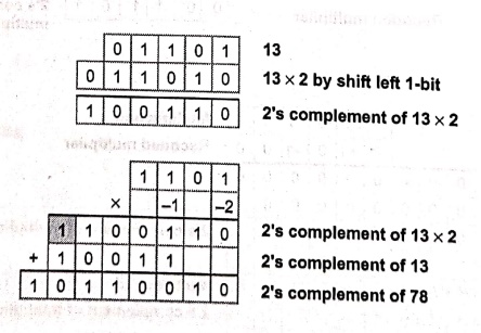
(+13) × (‒6) = (10110010)2 = (‒78)10
Example for Practice
Example: 7
Illustrate multiplication of signed
2's complement numbers 01101 and 11010 using bit‒pairing of the multipliers.
2. Array Multiplier
•
The multiplication process for binary numbers is similar to the decimal
numbers.
•
Actually binary multiplication is simple than decimal multiplication since it
involves only 1s and 0s.
Rules for binary
multiplication
■
0 × 0 = 0
■
1 × 0 = 0
■
0 × 1 = 0
■
1 × 1 = 1
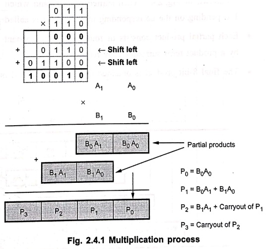
Example: 8
Multiply 0112 by 1102
using binary multiplication method.
Solution :
•
For multiplication in binary numbers, it uses n shifts and adds to multiply n‒bit
binary number.
•
The combination logic circuit implemented to perform such multiplication is called
combinational multiplier or array multiplier.
•
Let us generalize the multiplication process for a 2 x 2 multiplier for two
unsigned 2‒bit numbers: multiplicand A = A1A0 and
multiplier B = B1B0.
•
Fig. 2.4.1 shows how the multiplication process is carried out.
•
The multiplication process involves multiplication (product) of 2‒bit number
and addition of 2‒bit number.
•
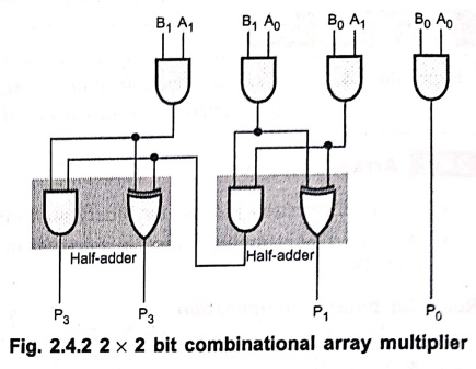
The multiplication of 2‒bits can be implemented using 2‒input AND gate whereas
addition of 2‒bits can be implemented using half‒adder. Such an implementation of
2x2 multiplier is shown
•
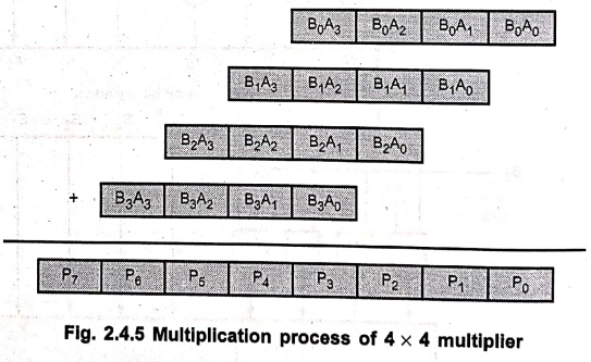
Fig. 2.4.2 shows the multiplication process for a 4 x 4 multiplier for two
unsigned integers multiplicand A = A3 A2 A1 A0 and multiplier B = B3
B2 B1 B0.
•
As shown in Fig. 2.4.3, each shifted multiplicand which is multiplied by either
0 or 1 depending on the corresponding multiplier bit is called partial product.
•
Each partial product consists of four product component. The product is
represented by a product term surrounded by rectangular box.
•
The final 8‒bit product is obtained by adding all partial products.
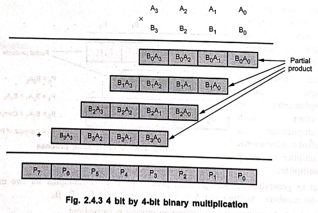
• The first partial product is formed by multiplying B0 by A3 A2 A1 A0. The second partial product is formed by multiplying B1 by A3 A2 A1 A0. The third partial is formed by multiplying B2 by A3 A2 A1 A0 and the fourth partial product is formed by multiplying B3 by A3 A2 A1 A0.
•
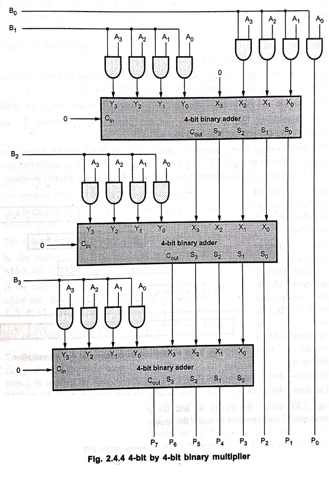
The multiplication of two bits such as B0 and A0 produces
a 1 if both bits are 1; otherwise, it produces a 0. This is identical to AND
operation. Therefore, the partial products can be implemented with AND gates as
shown in Fig. 2.4.4.
•
The 4‒bit partial products are added using 4‒bit parallel adder. During
addition of first partial product, three most significant bits of it are added
to the second partial product. As we take only three bits from first partial
product, the fourth (most significant bit) is considered as 0. This is
illustrated in Fig. 2.4.4.
•
The three most significant bits and carry out (treated as most significant bit)
of first partial sum are then added to the third partial product.
•
Finally the three most significant bits and carry out (treated as most
significant bit) of second partial sum are added to the fourth partial product.
•
The carryout and third sum represents the five most significant bits of the
product.
•
Least significant bits of first and second partial sum represents P1
and P2, respectively, and product B0A0
represents P0.
•
The 4‒bit by 4‒bit binary multiplier circuit discussed above can be drawn using
full adders as shown in Fig. 2.4.5, each shifted multiplicand which is
multiplied by either 0 or 1 depending on the corresponding multiplier bit is
called partial product.
•
Each product partial consists of four product component.
•
The product component bit is a logical AND of multiplier bit Bi and
multiplicand bit Aj, i.e. Bi× Aj and it is represented
by a product term surrounded by rectangular box.
•
The final 8‒bit product is obtained by adding all partial products.
•
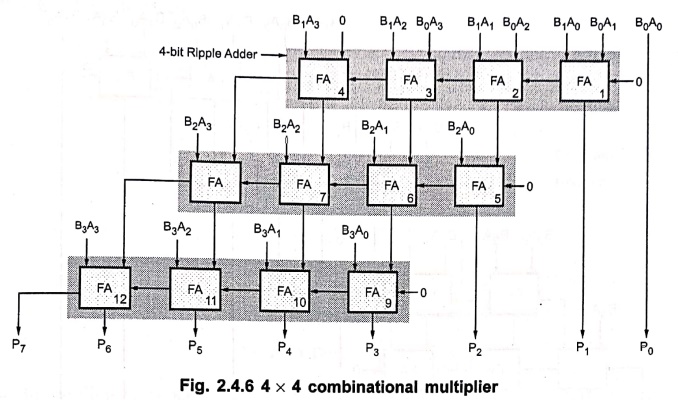
Fig. 2.4.6 shows the circuit to add the product components. Here, the product
components are separated to make the space, and each '+' box is a full adder.
•
The carries in each partial product row of full adders are connected to make an
4‒bit ripple adder. Thus, the first 4‒bit ripple adder adds the first two rows
of product components to produce the first partial product.
•
The carry output generated is propagated to the most significant product
component used to produce the next partial product.
•
The subsequent adders adds each partial product with the next product
component.
•
In the above multiplier, the least significant adder is full‒adder 1 and the
adder which gives the MSB of the product (P7) is full‒adder 12.
•
If we assume for simplicity that the delays from any input to any output of a
full adder are equal, say tpd, then the worst‒case path goes through
8 full‒adders (1, 2, 3, 4, 7, 8, 11 and 12) and its delay is 8 tpd.
3. Carry Save Multiplier
•
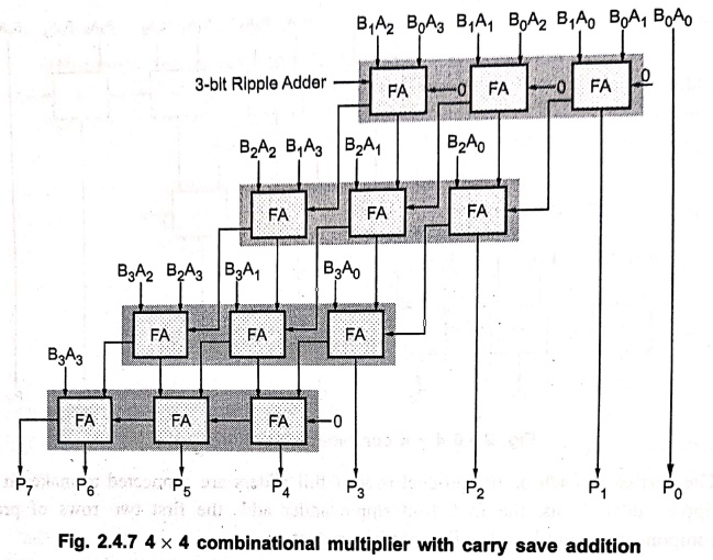
To increase the speed of the addition process many times technique called carry‒save addition is used. In this
technique, the carry output from bit i during step j is applied to carry input
for bit i + 1 during the next step, j + 1. After addition of product components
in the last row, one more step is required in which the carries are allowed to
ripple from the least to the most significant bit.
•
Fig. 2.4.7 shows 4 x 4 combinational multiplier using carry‒save addition
technique. In this the carry out of each full adder in the first seven row of
full adders are connected to an input of an adder below it. Carries in the
fourth row of full adders are connected to create a conventional ripple adder.
This technique does not save any hardware but it reduces the propagation delay
substantially.
Review Questions
1. Explain the
modified Booth's algorithm.
2. What is bit‒pair
recoding?
3. Carry out bit pair
recoding of following multipliers
1 1 0 1 0
0 1 1 0 1.
4. Design an array
multiplier that multipliers two 4 bit numbers. Use AND gates and binary
address.
5. Draw and explain 2‒bit
by 2‒bit array multiplier.
6. Explain the concept
of carry save addition for the multiplication operation, M × Q = P for 4‒bit
operands, with diagram and suitable example.
7. Write a note on the
carry‒save multiplier.
Computer Organization and Architecture: Chapter 2: Arithmetic for Computers : Tag: Computer : Arithmetic for Computers - Fast Multiplication
Computer Organization and Architecture: Chapter 2: Arithmetic for Computers
Under Subject
Computer Organization and Architecture
CW25201 3rd Semester IT department. | 2025 Regulation | 3rd Semester 2025 Regulation
Related Subjects
Discrete Mathematics
MA25C14 3rd Semester CSE,IT,CY,AIDS departments. | 2025 Regulation | 3rd Semester 2025 Regulation
Data Structures
CS25C08 3rd Semester CSE,IT,CY,AIDS departments. | 2025 Regulation | 3rd Semester 2025 Regulation
Computer Organization and Architecture
CW25201 3rd Semester IT department. | 2025 Regulation | 3rd Semester 2025 Regulation
Object Oriented Programming
CS25C07 3rd Semester IT department. | 2025 Regulation | 3rd Semester 2025 Regulation
Web Technologies
IT25301 3rd Semester IT department. | 2025 Regulation | 3rd Semester 2025 Regulation
English Communication Skills Laboratory I
EN25C03 3rd Semester all department. | 2025 Regulation | 3rd Semester 2025 Regulation
Skill Development Course I
3rd Semester all department. | 2025 Regulation | 3rd Semester 2025 Regulation