Electron Devices: Chapter 4: Bipolar Junction Transistors
Common Emitter CE Transistor Configuration
Bipolar Junction Transistors (BJT)
Common Emitter Configuration: i. Current Relations in CE Configuration ii. Input Characteristics (Base Curves) iii. Output Characteristics (Collector Curves) , iv) Important Example Solved Problems
CB, CE and CC Transistor Configurations
The transistor can be connected in a circuit in the following three configurations.
1. Common base configuration.
2. Common emitter configuration.
3. Common collector configuration.
Key Point: Regardless of circuit configuration, the base emitter junction is always forward biased while the collector‒base junction is always reverse biased, to operate transistor in active region.
2. Common Emitter Configuration
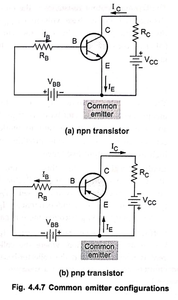
• In this configuration input is applied between base and emitter, and output is taken from collector and emitter.
• Here, emitter of the transistor is common to both, input and output circuits, and hence the name common emitter configuration.
• Common emitter configurations for both npn and pnp transistors are shown in Fig. 4.4.7 (a) and 4.4.7 (b), respectively.
• The input voltage in the CE configuration is the base‒emitter voltage (VBE) and the output voltage is the collector‒emitter voltage (VCE). The input current is IB and the output current is IC.
i. Current Relations in CE Configuration
• In configuration we have seen that
IC = αdcIE + ICBO
IC‒ICBO = αdcIE
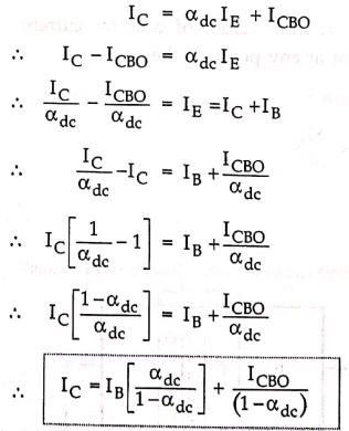
... (4.4.4)
• The βdc is the ratio of output current IC and input current IB in common emitter configuration. It is common emitter amplification factor or current gain.
It is given by,
βdc = IC/IB
We know that, β = IC/IB
We have,
IE = IC + IB
i.e., IB = IE ‒ IC
β = IC / [IE ‒ IC]
Dividing the numerator and denominator of R.H.S. of above equation by IE, we get,
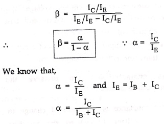
Dividing the numerator and denominator of R.H.S. of above equation by IB, we get,
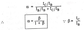
α = β / [1 + β]
Ex. 4.4.2: Calculate the collector and emitter current levels for a BJT with αdc = 0.99 and IB = 20 μA
Solution: :
Bdc = αdc / (1 ‒ αdc)
= 0.99 / (1‒0.99)
= 99
IC = βdc IB = 99×20 μA = 1.98 mA
IE = IC+IB = 1.98 mA + 20 μA = 2 mА
Ex. 4.4.3: Calculate the values of IC and IE for a BJT with αdc = 0.97 and IB = 50 μA. Determine βdc for the device.
Solution: :
Bdc = αdc / (1 ‒ αdc)
= 0.97 / (1‒0.97)
= 32.33
IC = βdc IB = 32.33 × 50 μA = 1.6165 mA
IE = IB + IC = 50 μA + 1.6165 mA
= 1.6665 mA
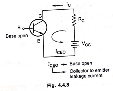
ICEO
From equation (4.4.4) we have,
IC = [αdc / 1‒αdc ]IB + (ICBO / 1‒αdc )
IC = βdcIB + (1+βdc)ICBO
………….(4.4.5)
Since
1+ βdc = 1 + (αdc / 1‒αdc)
= [ 1 ‒αdc + αdc ] / [ 1‒αdc ]
= 1 / ( 1‒αdc )
The terms (1 + βdc) ICBO in equation (4.4.5) is denoted as ICEO and is the reverse saturation current for the CE configuration.
(1+βdc)ICBO = ICEO
IC = βdcIB + ICEO
Ex. 4.4.4: The reverse leakage current of the transistor when connected in CB configuration is 0.2 μA and it is 18 μA when same transistor is connected in CE configuration. Calculate αdc and βdc of the transistor. (Assume IB = 30 mA)
Solution:
Given: ICBO = 0.2 μA, ICEO = 18 μA
ICEO = (1 + βdc)ICBO
(1 + βdc) = ICEO / ICEO = 18 μA / 0.2 μA = 90
βdc = 89
αdc = βdc / (1 + βdc)
= 89 / (1+89) = 0.989
Ex. 4.4.5: Calculate the αdc and βac for the given transistor for which IC=5 mA, IB =50 μA and ICO = 1 μΑ.
Solution:
IC=5mA, IB = 50 μA, ICO =ICBO = 1 μA
IC = βdcIB +(1+βdc)ICBO
5×10‒3 = βdc × 50×10−6 + (1+βdc)×1×10‒6
5×10‒3 ‒ 1×10‒6 = 51×10‒6 βdc
βdc = 4.999×10‒3 / 51×10‒6 = 98
αdc = βdc / (1+ βdc) = 98 / (1+98) = 0.9899
Ex. 4.4.6: A transistor has β = 150, find the collector and base current, if IE = 10 mA.
Solution:
IB = IE / (1+β) = 10mA / (1+150) = 66.225 μA
IC = βIB = 150×66225 μA = 9.934 mA
Ex. 4.4.7: A transistor with IB = 100 μA and IC = 2 mA find
1) β of the transistor
2) α of the transistor
3) Emitter current IE
4) If IB changes by 25μA and IC changes by 0.6 mA. Find the new value of β.
Solution: :
1) β = IC/IB
= 2×10‒3 / 100×10‒6
= 20
2) α = β / (1+β)
= 20 / (1+20) = 0.9524
3) IE = IB + IC = 100×10‒6 + 2×10‒3 = 2.1 mA
4) New value of IB = 100 + 25 = 125 mA
New value of IC = 2 + 0.6 = 2.6 mA
New value of β = 2.6×10‒3 / 125×10‒6
= 20.8
ii. Input Characteristics (Base Curves)
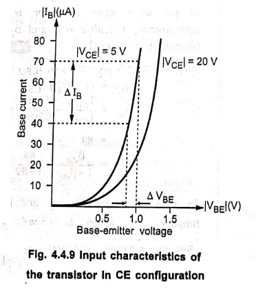
• It is the curve between and input voltage VBE (base‒emitter voltage) and input current IB (base current) at constant collector‒emitter voltage, VCE: The base current is taken along Y‒axis and base emitter voltage VBE is taken along X‒axis.
• Fig. 4.4.9 shows the input characteristics of a typical transistor in common‒emitter configuration.
From characteristics we observe the following important points:
1. The input resistance is the ratio of change in base‒emitter voltage (ΔVBE) to the resulting change in base current (ΔIB) at constant collector emitter voltage VCE. It is given by,
Note: While plotting input characteristics the magnitudes of voltage and current are considered. Practically the voltage and current polarities are opposite for pnp and npn transistors
2. The value of r1 in CE configuration is greater than the value of r1 in CB configuration.
3. As the input to transistor in the CE configuration is between the base‒to‒emitter junction, the CE input characteristics resembles a family of forward biased diode curves.
4. After the cut‒in voltage, the base current (IB) increases rapidly rapidly with small increase base‒emitter voltage (VBE). Thus the dynamic input resistance is small in CE configuration.
5. For a fixed value of VBE, IB decreases as VCE is increased.
6. Voltages VBE and VCE are positive for npn transistor and they are negative for pnp transistor.
iii. Output Characteristics (Collector Curves)
From this characteristics we observe the following important points:
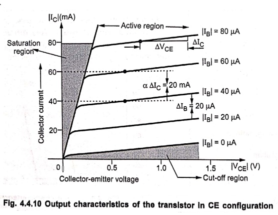
1. This characteristics shows the relation between the collector current IC and collector voltage VCE, for various fixed values of IB. This characteristics is often called collector characteristics. A typical family of output characteristics for an n‒p‒n transistor in CE configuration is shown in Fig. 4.4.10.
Note: While plotting output characteristics the magnitudes of voltage and current are considered. Practically the voltage and current polarities are opposite for pnp and npn transistors
2. The value of Bdc of the transistor can be found at any point on the characteristics by taking the ratio IC to IB at that point, i.e. βdc = IC/IB. This is known as D.C. beta for the transistor.
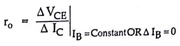
3. From the output characteristics, we can see that change in collector‒emitter voltage (ΔVCE) causes the little change in the collector current (ΔIC) for constant base current IB. Thus the output dynamic resistance is high in CE configuration.
4. The output characteristics of common emitter configuration consists of three regions: Active, Saturation and Cut‒off.
Active region :
For the operation in the active region, the emitter‒base junction (JE) is forward biased while collector base junction (JC) is reverse biased.
The collector current rise more sharply with increasing VCE in the linear region of output characteristics of CE transistor.
Saturation region:
In this region, the emitter‒base junction (JE) and collector base junction (JC) both are forward biased. In this region, IC does not depend upon the input current IB.
The saturation value of VCE, designated VCE(sat), usually ranges between 0.1 V to 0.3 V.
Cut‒off region:
The region below IB = 0 is the cut‒off region of operation for the transistor. In this region, both the junctions of the transistor are reverse biased.
For saturation: IB > IC/βdc
For active region: VCE > VCE (sat)
DC current gain: βdc = β = IC/IB
AC current gain: 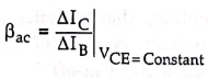
Electron Devices: Chapter 4: Bipolar Junction Transistors : Tag: electronics : Bipolar Junction Transistors (BJT) - Common Emitter CE Transistor Configuration
Electron Devices: Chapter 4: Bipolar Junction Transistors
Under Subject

Electron Devices
EC25C01 2nd Semester ECE Dept | 2025 Regulation | 2nd Semester 2025 Regulation
Related Subjects

English Essentials II
EN25C02 2nd Semester | 2025 Regulation | 2nd Semester 2025 Regulation

Tamils and Technology தமிழர்களும் தொழில்நுட்பமும்
UC25H02 2nd Semester | 2025 Regulation | 2nd Semester 2025 Regulation

Linear Algebra
MA25C02 2nd Semester | 2025 Regulation
Electron Devices
EC25C01 2nd Semester ECE Dept | 2025 Regulation | 2nd Semester 2025 Regulation

Data Structures using CPlusPlus
CS25C05 2nd Semester ECE Dept | 2025 Regulation | 2nd Semester 2025 Regulation

Circuits and Network Analysis
EC25C02 2nd Semester ECE Dept | 2025 Regulation | 2nd Semester 2025 Regulation

Re-Engineering for Innovation
ME25C05 2nd Semester | 2025 Regulation | 2nd Semester 2025 Regulation

Engineering Drawing - Laboratory
ME25C01 2nd Semester | 2025 Regulation | 2nd Semester 2025 Regulation

Data Structures using CPlusPlus - Laboratory
CS25C05 2nd Semester ECE Dept | 2025 Regulation | 2nd Semester 2025 Regulation

Devices and Circuits Laboratory
EC25C03 2nd Semester ECE Dept | 2025 Regulation | 2nd Semester 2025 Regulation