Electron Devices: Chapter 4: Bipolar Junction Transistors
Common Collector CC Transistor Configuration
Bipolar Junction Transistors (BJT)
i. Current Relations In CC Configuration ii. Common Collector Input Characteristics iii. Common Collector Output Characteristics
CB, CE and CC Transistor Configurations
The transistor can be connected in a circuit in the following three configurations.
1. Common base configuration.
2. Common emitter configuration.
3. Common collector configuration.
Key Point: Regardless of circuit configuration, the base emitter junction is always forward biased while the collector‒base junction is always reverse biased, to operate transistor in active region.
3. Common Collector Configuration
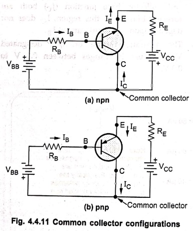
• In this configuration, input is applied between base and collector and output is taken from emitter and collector.
• Here, collector of the transistor is common to both input and output circuits and hence the name common collector configuration. It is also known as emitter follower configuration.
• Common collector connections for both npn and pnp transistors are shown in Fig. 4.4.11 (a) and 4.4.11 (b), respectively.
i. Current Relations In CC Configuration
We know that
IE = IB + IC
= IB + αdc1E + ICBO
IE(1‒αdc) = IB +ICBO
IE = IB/(1‒αdc) + ICBO/(1‒αdc)
We know that
βdc = αdc / (1‒αdc)
1+ βdc = 1+ [ αdc / (1‒αdc) ]
= [ 1‒αdc + αdc ] / (1‒αdc)
= 1 / (1‒αdc)
IE = IB(1+βdc) + ICBO(1+βdc)
Neglecting ICBO we have
IE = IB (1+ βdc)
Current gain in CC configuration is given by
γ = IE/IB = (1+ βdc)
= 1 + αdc/(1‒αdc)
= 1 / (1‒αdc)
ii. Common Collector Input Characteristics
• The input characteristics of CC configuration is a graph of input current IB (base current) versus input voltage VCB (collector base voltage) at constant VCE.
• The base current is taken along Y‒axis and collector base voltage VCB is taken along X‒axis.
• Fig. 4.4.12 shows the input characteristics of a typical transistor in common‒collector configuration.
• The common collector input characteristics are quite different from either common base or common emitter input characteristics. This difference is due to the fact that the input voltage VCB is largely determined by the level of collector to emitter voltage VCE.
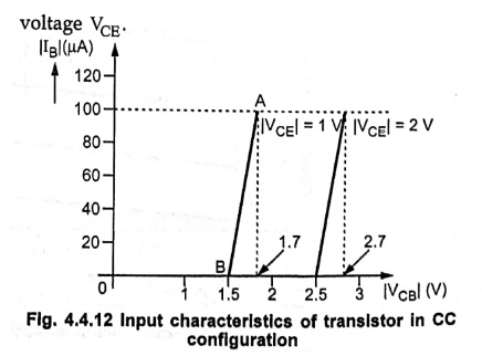
Fig. 4.4.12 Input characteristics of transistor in CC configuration
• Looking at Fig. 4.4.12 we can write,
VCE = VCB ‒ VBE
Or
VCB = VCE + VBE
• In CC configuration input junction is BC and it is reversed biased so input resistance in CC configuration is very high.
iii. Common Collector Output Characteristics
• It is the curve between emitter current IE and collector to emitter voltage VCE at constant base current IB.
• The emitter current is taken along Y‒axis and collector to emitter voltage along X‒axis.
• Fig. 4.4.13 shows the output characteristics of a typical transistor in common collector configuration.
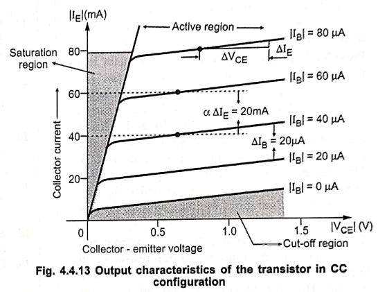
Fig. 4.4.13 Output characteristics of the transistor in CC configuration
• Since, IC is approximately equal to IE, the common collector output characteristics are practically similar to those of the common emitter output characteristics.
Electron Devices: Chapter 4: Bipolar Junction Transistors : Tag: electronics : Bipolar Junction Transistors (BJT) - Common Collector CC Transistor Configuration
Electron Devices: Chapter 4: Bipolar Junction Transistors
Under Subject

Electron Devices
EC25C01 2nd Semester ECE Dept | 2025 Regulation | 2nd Semester 2025 Regulation
Related Subjects

English Essentials II
EN25C02 2nd Semester | 2025 Regulation | 2nd Semester 2025 Regulation

Tamils and Technology தமிழர்களும் தொழில்நுட்பமும்
UC25H02 2nd Semester | 2025 Regulation | 2nd Semester 2025 Regulation

Linear Algebra
MA25C02 2nd Semester | 2025 Regulation
Electron Devices
EC25C01 2nd Semester ECE Dept | 2025 Regulation | 2nd Semester 2025 Regulation

Data Structures using CPlusPlus
CS25C05 2nd Semester ECE Dept | 2025 Regulation | 2nd Semester 2025 Regulation

Circuits and Network Analysis
EC25C02 2nd Semester ECE Dept | 2025 Regulation | 2nd Semester 2025 Regulation

Re-Engineering for Innovation
ME25C05 2nd Semester | 2025 Regulation | 2nd Semester 2025 Regulation

Engineering Drawing - Laboratory
ME25C01 2nd Semester | 2025 Regulation | 2nd Semester 2025 Regulation

Data Structures using CPlusPlus - Laboratory
CS25C05 2nd Semester ECE Dept | 2025 Regulation | 2nd Semester 2025 Regulation

Devices and Circuits Laboratory
EC25C03 2nd Semester ECE Dept | 2025 Regulation | 2nd Semester 2025 Regulation