Electron Devices: Chapter 4: Bipolar Junction Transistors
Bipolar Junction Transistors (BJT): Two Marks Important Questions and Answers
Electron Devices
Electron Devices: Chapter 4: Bipolar Junction Transistors : Anna University Part A Two Marks Important Questions and Answers
Electron
Devices
Chapter
4: Bipolar Junction Transistors
Two Marks
Questions with Answers
1. What is transistor?
Transistor
is a three terminal device : Base, emitter and collector, can be operated in
three configurations common base, common emitter and common collector.
According to configuration it can be used for voltage as well as current
amplification.
2. What are the terminals
present in a transistor?
Three
terminals: emitter, base, collector.
3. State the two types of
transistors.
There
are two types of transistors : Unipolar junction transistor and Bipolar
junction transistor.
4. Why transistor is also
called bipolar junction transistor ?
The
current conduction in bipolar transistor is because of both the types of charge
carriers, holes and electrons. Hence this is called Bipolar junction
transistor.
5. Why transistor called a
current controlled device ?
In
BJT output current is controlled by input current and hence it is a current
controlled device.
6. Mention the types of
BJT.
The
types of BJT are : 1. n‒p‒n type 2. p‒n‒p type
7. State the two junctions
in the transistor.
A
transistor has two p‒n junctions. One junction is between the emitter and the
base and is called the emitter base junction or simply the emitter junction JE.
The other junction is between the base and the collector and and is called
collector‒base junction or simply collector junction JC.
8. What is doping?
The
process by which impurities are added to a pure semiconductor is called doping.
9. Explain about the doping
in transistor.
The
base region is very thin and lightly doped. The emitter and collector are
heavily doped. But the doping level in emitter is slightly greater than that of
collector.
10. State the basic
currents of the transistor.
The
basic currents of the transistor are: base current, collector current and
emitter current. They are related by equation IE = IB + IC
11. Define αdc
and βdc
αdc is the fraction of IE
that crosses over from emitter to the collector region.
βac is defined as the ratio of the
collector current to the base current.
12. Give the relation
between αdc and βdc
β = α / (1‒α)
and α = β / (1+β)
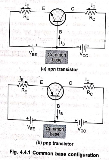
13. Draw the neat circuit
configuration of CB.
14. What is the
characteristics of a transistor?
Input
characteristics: It is the relationship plotted
graphically between input voltage and input current while keeping output voltage
as constant.
Output
characteristics: It is the relationship plotted
graphically between the output voltage and output current while keeping input
current as constant.
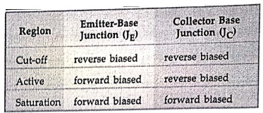
15. State the three
operating regions of transistor.
The
three operating regions of transistor are Active, cut‒off and saturation.
16. State the relation
between operating region and biasing of transistor junctions.
The
table gives the relation between operating region and biasing biasing of
transistor junctions.
17. When does a transistor
act as a switch?
The
transistor acts as a switch when it is operated at either cutoff region or
saturation region.
18. What is early effect?
When
reverse bias voltage VCB increases, the width of depletion region
also increases, which reduces the electrical base width. This effect is called
as 'Early effect' or 'Base width modulation'.
19. What is a multi‒emitter
transistor ?
A
multi‒emitter transistor is a type of Bipolar Junction Transistor (BJT) that
has more than one emitter terminal. Each emitter acts as a separate input,
allowing the transistor to accept multiple logic signals simultaneously. It is
mainly used in Transistor‒Transistor Logic (TTL) circuits.
20. What is the primary
application of a multi‒emitter transistor?
The
primary application of a multi‒emitter transistor is in the input stage of TTL
logic gates, especially NAND gates. It replaces multiple diodes used in earlier
logic families (like DTL), providing faster switching speed and compact circuit
design.
21. Why is a multi‒emitter
transistor preferred in TTL circuits ?
It
is preferred because each emitter can serve as a separate input terminal,
enabling multi‒input logic operations within a single transistor. This reduces
the number of components, minimizes propagation delay and switching speed in
digital ICs.
Electron Devices: Chapter 4: Bipolar Junction Transistors : Tag: electronics : Electron Devices - Bipolar Junction Transistors (BJT): Two Marks Important Questions and Answers
Electron Devices: Chapter 4: Bipolar Junction Transistors
Under Subject

Electron Devices
EC25C01 2nd Semester ECE Dept | 2025 Regulation | 2nd Semester 2025 Regulation
Related Subjects

English Essentials II
EN25C02 2nd Semester | 2025 Regulation | 2nd Semester 2025 Regulation

Tamils and Technology தமிழர்களும் தொழில்நுட்பமும்
UC25H02 2nd Semester | 2025 Regulation | 2nd Semester 2025 Regulation

Linear Algebra
MA25C02 2nd Semester | 2025 Regulation
Electron Devices
EC25C01 2nd Semester ECE Dept | 2025 Regulation | 2nd Semester 2025 Regulation

Data Structures using CPlusPlus
CS25C05 2nd Semester ECE Dept | 2025 Regulation | 2nd Semester 2025 Regulation

Circuits and Network Analysis
EC25C02 2nd Semester ECE Dept | 2025 Regulation | 2nd Semester 2025 Regulation

Re-Engineering for Innovation
ME25C05 2nd Semester | 2025 Regulation | 2nd Semester 2025 Regulation

Engineering Drawing - Laboratory
ME25C01 2nd Semester | 2025 Regulation | 2nd Semester 2025 Regulation

Data Structures using CPlusPlus - Laboratory
CS25C05 2nd Semester ECE Dept | 2025 Regulation | 2nd Semester 2025 Regulation

Devices and Circuits Laboratory
EC25C03 2nd Semester ECE Dept | 2025 Regulation | 2nd Semester 2025 Regulation