Electron Devices: Chapter 4: Bipolar Junction Transistors
Common Base CB Transistor Configuration
Bipolar Junction Transistors (BJT)
Common base configuration: i. Current Relations in CB Configuration ii. Input Characteristics (Base Curves) iii. Output Characteristics (Collector Curves) iv. Early Effect
CB, CE and CC Transistor Configurations
The transistor can be connected in a circuit in the following three configurations.
1. Common base configuration.
2. Common emitter configuration.
3. Common collector configuration.
Key Point: Regardless of circuit configuration, the base emitter junction is always forward biased while the collector‒base junction is always reverse biased, to operate transistor in active region.
1. Common Base Configuration
• To understand complete electrical behaviour of a transistor it is necessary to study the interrelation of the various currents and voltages. These relationships can be plotted graphically which are commonly known as the characteristics of transistor.
• The most important characteristics of transistor in any configuration are input and output characteristics.
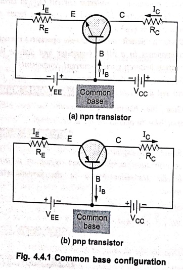
• Fig. 4.4.1 shows the common base configuration. As shown in Fig. 4.4.1, in this configuration input is applied between emitter and base and output is taken from the collector and base.
• Here, base of the transistor is common to both input and output circuits and hence the name common base configuration.
• Common base configurations for both npn and pnp transistors are shown in Fig. 4.4.1 (a) and 4.4.1 (b), respectively.
i. Current Relations in CB Configuration
• In common base configuration, the collector current IC is given by,
IC = IC(INJ) + ICBO
... (4.4.1)
IC(INJ): It is an injected collector current due to number of electrons crossing the collector base junction.
ICBO: It is the reverse saturation current flowing due to the minority carrier between collector and base when the emitter is open. ICBO is negligible as compared to IC(INJ) and therefore we have
IC = IC(INT)
However, when emitter is open
IC = ICBO
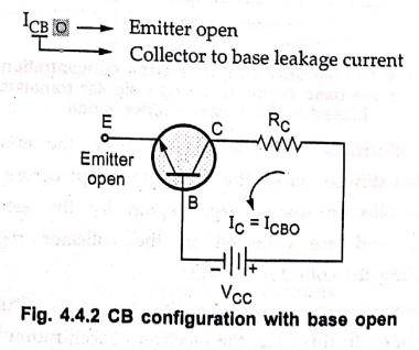
Key Point: The reverse saturation current, ICBO, is temperature sensitive and it doubles for every 10°C rise in temperature.
Current Application Factor (αdc)
αdc: It is defined as the ratio of the collector current resulting from carrier injection to the total emitter current.
αdc = α = IC(INJ) / IE
……………..(4.4.2)
Since IC < IE the value of αdc is always less than unity. It ranges from 0.95 to 0.995 depending on the thickness of the base region; larger the thickness of the base, smaller is the value of αdc. It represents the current gain in the CB configuration.
Substituting the value of IC(INJ) in equation (4.4.2)
we have
IC = αdcIE +ICBO
………..(4.4.3)
However, ICBO is negligibly small
IC = αdcIE
Current amplification factor in CB
αdc = IC / IE
IB in terms of αdc
We know that
IE = IB + IC
IB = IE‒IC
= IE ‒ (αdcIE + ICBO)
= IE ‒ αdcIE
ICBO → 0
IB = (1 ‒ αdc) IE
Ex. 4.4.1: Given IE = 2.5 mA, α = 0.98 and ICBO = 10 μA calculate IB and Ic.
Solution:
IC = αIE + ICBO
= 0.98 × 2.5 × 10‒3 + 10×10‒6 = 2.46 mA
IB = IE‒IC = 2.5×10³ − 2.46×10−3 = 40 μA
ii. Input Characteristics (Base Curves)
• It is the curve between an input voltage VEB (emitter‒base voltage) and input current IE (emitter current) at constant collector‒base voltage VCB. The emitter current is taken along Y‒axis and emitter base voltage along X‒axis.
• Fig. 4.4.3 shows the input characteristics of a typical transistor in common‒base configuration.
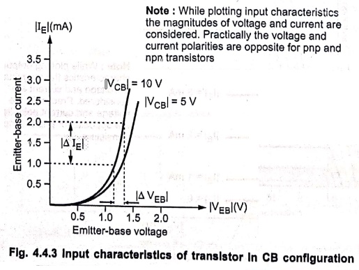
Note: While plotting input characteristics the magnitudes of voltage and current are considered. Practically the voltage and current polarities are opposite for pnp and npn transistors
From this characteristics we can observe the following important points:
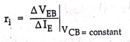
1. The input resistance is a ratio of change in emitter‒base voltage (ΔVEB) to the resulting change in emitter current (ΔIE) at constant collector‒base voltage (VCB).
It is given by
2. After the cut‒in voltage (barrier potential, normally 0.7 V for silicon and 0.3 V for germanium), the emitter current (IB) increases rapidly with small increase in emitter‒base voltage (VEB). Thus, the input resistance is very small.
3. It can be observed that there is slight increase in emitter current (IE) with increase in VCB. This is due to change in the width of the depletion region in the base region under the reverse biased condition.
4. VCB is positive for npn transistor and it is negative for pnp transistor. On the other hand VEB is negative for npn transistor and it is positive for pnp transistor.
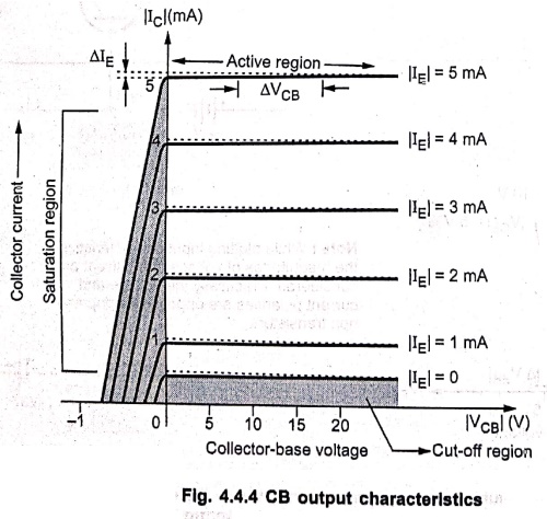
Note: While plotting output characteristics the magnitudes of voltage and current are considered. Practically the voltage and current polarities are opposite for pnp and npn transistors
iii. Output Characteristics (Collector Curves)
• It is the curve between collector current IC and collector base voltage VCB at constant emitter current IE. The collector current is taken along Y‒axis and collector‒base voltage magnitude along X‒axis. Fig. 4.4.4 shows the output characteristics of a typical transistor in common base configuration.
From this characteristics we observe following points :
The output characteristics has three basic regions : Active, cut‒off and saturation.
• Active region :
• For the operation in the active region, the emitter‒base junction (JE) is forward biased while collector base junction (JC) is reverse biased.
• In this region, collector current IC is approximately equal to the emitter current (IE) and transistor works as an amplifier.
• In the active region, the collector current is essentially almost constant.
• The Dynamic output resistance is the ratio of change in collector base voltage (ΔVCB) to the resulting change in collector current (ΔIC) at constant emitter current (IE). It is given by
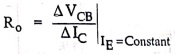
• The collector current IC is almost independent on collector‒base voltage VCB and the transistor can be said to work as constant‒current source. This provides very high dynamic output resistance.
• Saturation region : In this region, the emitter‒base junction (JE) and collector base junction (JC) both are forward biased (VCB is negative). Here, the IC is independent of IE. IC decreases rapidly as VCB becomes more negative.
• Cut‒off region: The region below the curve IE = 0 is known as cut‒off region, where the collector current is nearly zero and the collector‒base (JC) and emitter‒base (JE) junctions of a transistor are reverse biased.
• DC current gain :
αdc = α = IC/IE
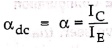
where IC and IE are the values of collector current and emitter current at any point on the curve.
• AC current gain :
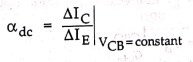
iv. Early Effect
• As shown in Fig. 4.4.5, the width of the base region occupied by charge particles is known as electrical width or physical width of the base region.
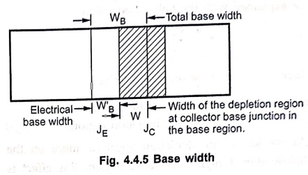
• Since doping in the base is ordinarily substantially smaller than that of the collector, the penetration of the transition region into the base is much larger than into the collector. Hence the base depletion region is large.
• Here, when reverse bias voltage VCB increases, the width of depletion region in base region also increases, which reduces the electrical base width (W'B).
• Due to reduction of the electrical base width, now there are more charge particles per unit area. In other words, due to reduction of the electrical base of width, concentration the charge gradient increases in the base region. This increase in concentration of charge carriers causes more diffusion of electrons from n‒type emitter to p‒type base increasing emitter current slightly.
• The increase in reverse bias voltage VCB, the width of depletion region increases, which reduces the electrical base width. This effect is called as 'Early Effect' or 'Base width modulation'. This effect can be explained with the help of equation
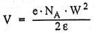
V = [ e. NA . W2 ] / 2ε
where
V = Reverse bias voltage.
and
W = Width of the space‒charge region/depletion region.
• As we know, the depletion width is more on the lightly doped region, i.e. base region, this effect is more in the base region reducing the effective (electrical) base width.
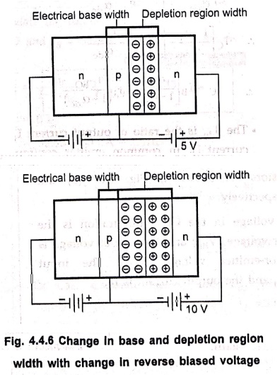
• This decrease in base width has two consequences.
1. There is less chance for recombination within the base region. Hence the transport factor β* and also αr increase with an increase in the magnitude of the collector junction voltage.
2. The charge gradient is increased within the base and consequently, the current of minority carriers injected across the junction increases.
Electron Devices: Chapter 4: Bipolar Junction Transistors : Tag: electronics : Bipolar Junction Transistors (BJT) - Common Base CB Transistor Configuration
Electron Devices: Chapter 4: Bipolar Junction Transistors
Under Subject

Electron Devices
EC25C01 2nd Semester ECE Dept | 2025 Regulation | 2nd Semester 2025 Regulation
Related Subjects

English Essentials II
EN25C02 2nd Semester | 2025 Regulation | 2nd Semester 2025 Regulation

Tamils and Technology தமிழர்களும் தொழில்நுட்பமும்
UC25H02 2nd Semester | 2025 Regulation | 2nd Semester 2025 Regulation

Linear Algebra
MA25C02 2nd Semester | 2025 Regulation
Electron Devices
EC25C01 2nd Semester ECE Dept | 2025 Regulation | 2nd Semester 2025 Regulation

Data Structures using CPlusPlus
CS25C05 2nd Semester ECE Dept | 2025 Regulation | 2nd Semester 2025 Regulation

Circuits and Network Analysis
EC25C02 2nd Semester ECE Dept | 2025 Regulation | 2nd Semester 2025 Regulation

Re-Engineering for Innovation
ME25C05 2nd Semester | 2025 Regulation | 2nd Semester 2025 Regulation

Engineering Drawing - Laboratory
ME25C01 2nd Semester | 2025 Regulation | 2nd Semester 2025 Regulation

Data Structures using CPlusPlus - Laboratory
CS25C05 2nd Semester ECE Dept | 2025 Regulation | 2nd Semester 2025 Regulation

Devices and Circuits Laboratory
EC25C03 2nd Semester ECE Dept | 2025 Regulation | 2nd Semester 2025 Regulation