Electron Devices: Chapter 4: Bipolar Junction Transistors
Construction of pnp and npn Transistors
Bipolar Junction Transistors (BJT)

Questions: 1. Why collector region of a transistor is larger in area than emitter region? 2. Explain the construction of n‒p‒n and p‒n‒p transistors. 3. Why transistor can not be replaced by back to back diode connection? 4. Explain the terms emitter, collector and base. 5. Sketch the symbols of transistors.
Construction
of pnp and npn Transistors
•
When a transistor is formed by sandwiching a single p‒region between two n‒regions,
as shown in Fig. 4.2.1 (a), it is an n‒p‒n type transistor. The p‒n‒p type
transistor has a single n‒region between two p‒regions, as shown in Fig. 4.2.1
(b).
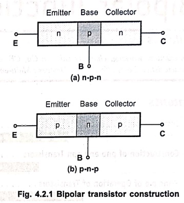
Fig. 4.2.1 Bipolar
transistor construction
•
The middle region of each transistor type is called the base of the transistor.
This region is very thin and lightly doped.
•
The process by which impurities are added to a pure semiconductor is called
doping.
•
The remaining two regions are called emitter and collector.
•
The emitter and collector are heavily doped. But the doping level in emitter is
slightly greater than that of collector.
•
The collector region‒area is slightly more than that of emitter. It helps in
better power dissipation.
Transistor Symbols
•
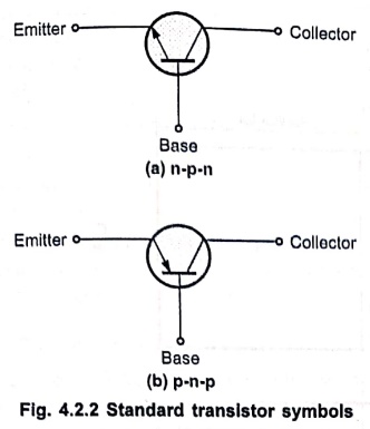
Fig. 4.2.2 (a) and (b) shows the symbols of and pnp transistors. Arrowhead on a
transistor symbol indicates the conventional current which is opposite to the
direction of electron current in emitter.
Diode Equivalent Structure of Transistor
•
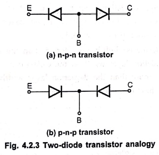
A transistor can be considered as two p‒n junction diodes connected back to
back as shown in Fig. 4.2.3 (a) and (b).
Junctions of Transistor
•
A transistor has two p‒n junctions.
•
One junction is between the emitter and the base and is called the emitter base
junction or simply the emitter junction JE.
•
The other junction is between the base and the collector and is called collector‒base
junction or simply collector junction JC.
Cannot Replace Transistor by Back to Back Diodes
•
However, we cannot replace transistor by back to back connected diodes because
of the following reasons:
1.
Relative doping levels in the base, emitter and collector junctions must be
satisfied to work that device as a transistor. Two normal p‒n junction diodes
cannot satisfy this requirement.
2.
In a transistor, emitter to base junction is forward biased while base to
collector junction is reversed biased. But due to diffusion process almost
entire emitter current reaches to collector and base current is negligibly
small. Thus due to diffusion, device works as a transistor. While in back to
back connected diodes there are two separate diodes, one forward biased and one
reverse biased and diffusion cannot take place. Thus maximum series current
which can flow is reverse saturation current of a reverse biased diode. Hence
the combination of back to back connected diodes cannot be used as transistor.
•
Another important point is that, the emitter area in the transistor is
considerably smaller than the collector area. This is because the collector
region has to handle more power than the emitter and more surface area is
required for heat dissipation.
Review Questions
1. Why collector region of a transistor is larger in area than
emitter region?
2. Explain the construction of n‒p‒n and p‒n‒p transistors.
3. Why transistor can not be replaced by back to back diode
connection?
4. Explain the terms emitter, collector and base.
5. Sketch the symbols of transistors.
Electron Devices: Chapter 4: Bipolar Junction Transistors : Tag: electronics : Bipolar Junction Transistors (BJT) - Construction of pnp and npn Transistors
Electron Devices: Chapter 4: Bipolar Junction Transistors
Under Subject

Electron Devices
EC25C01 2nd Semester ECE Dept | 2025 Regulation | 2nd Semester 2025 Regulation
Related Subjects

English Essentials II
EN25C02 2nd Semester | 2025 Regulation | 2nd Semester 2025 Regulation

Tamils and Technology தமிழர்களும் தொழில்நுட்பமும்
UC25H02 2nd Semester | 2025 Regulation | 2nd Semester 2025 Regulation

Linear Algebra
MA25C02 2nd Semester | 2025 Regulation
Electron Devices
EC25C01 2nd Semester ECE Dept | 2025 Regulation | 2nd Semester 2025 Regulation

Data Structures using CPlusPlus
CS25C05 2nd Semester ECE Dept | 2025 Regulation | 2nd Semester 2025 Regulation

Circuits and Network Analysis
EC25C02 2nd Semester ECE Dept | 2025 Regulation | 2nd Semester 2025 Regulation

Re-Engineering for Innovation
ME25C05 2nd Semester | 2025 Regulation | 2nd Semester 2025 Regulation

Engineering Drawing - Laboratory
ME25C01 2nd Semester | 2025 Regulation | 2nd Semester 2025 Regulation

Data Structures using CPlusPlus - Laboratory
CS25C05 2nd Semester ECE Dept | 2025 Regulation | 2nd Semester 2025 Regulation

Devices and Circuits Laboratory
EC25C03 2nd Semester ECE Dept | 2025 Regulation | 2nd Semester 2025 Regulation