Electron Devices: Chapter 4: Bipolar Junction Transistors
Principle of Operation of Bipolar Junction Transistors (BJT)
Questions: 1. Explain various voltage components of transistor. 2. Explain the various current components of the transistor. 3. Write equations for collector current (IC) in terms of emitter current (IE) and αdc, and in terms of base current (IB) and αdc. 4. Draw a sketch to show the various current components in a NPN transistor and deduce the relation between various current components. 5. Sketch the symbols of transistors and mark the current directions. 6. Give the biasing arrangement for an NPN transistor to operate in the active region. 7. Sketch and explain the minority carrier electron concentration across the base region of an npn bipolar transistor biased in the forward‒active mode. 8. State expressions of IC, IE and IB. 9. What is the need for biasing in the transistor? 10. Describe the working of PNP transistor.
Principle
of Operation of Transistors
1. Unbiased Transistor
•
An unbiased transistor means a transistor with no external voltage (biasing) is
applied. Obviously, there will be no current flowing from any of the transistor
leads.
•
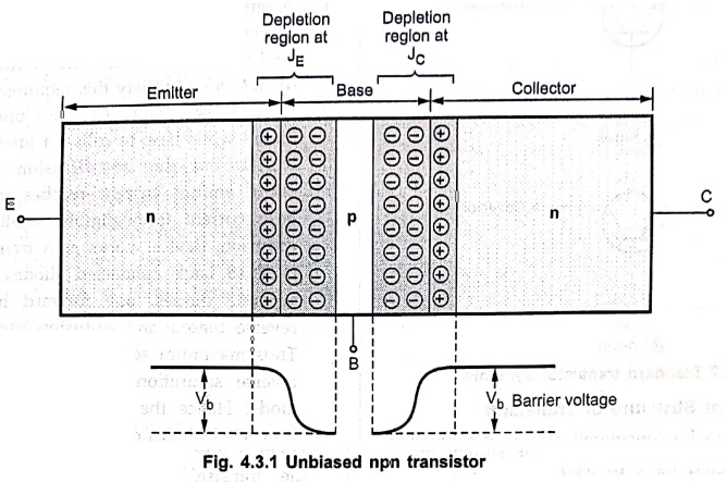
Since transistor is like two pn junction diodes connected back to back, there
are depletion regions at both the junctions, emitter junction and collector
junction, as shown in Fig. 4.3.1.
•
During diffusion process, depletion region penetrates more deeply into the
lightly doped side in order to include an equal number of impurity atoms in the
each side of the junction.
•
As shown in Fig. 4.3.1, depletion region at emitter junction penetrates less in
the heavily doped emitter and extends more in the base region.
•
Similarly, depletion region at collector junction penetrates less in the
heavily doped collector and extends more in the base region.
• As collector is slightly less doped than the emitter, the depletion layer width at the collector junction is slightly more than the depletion layer width at the emitter junction.
•
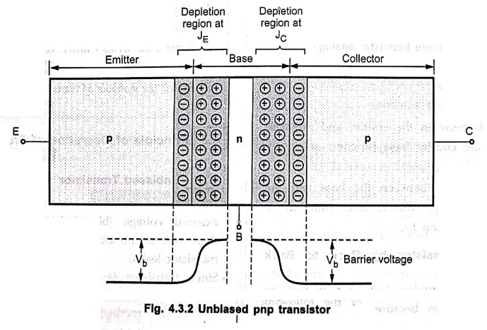
Barrier voltage is the voltage necessary to cause electrical conduction in a
junction of two dissimilar materials.
•
Like diodes, a barrier voltage exists within the transistor.
•
The barrier voltage at each junction is positive on the n‒side and negative on
p‒side.
•
The barrier voltage across the junction in a silicon. transistor is about 0.7
volt and approximately 0.3 volt in a germanium transistor.
2. Biased Transistor
The transistor can be operated in four possible bias combinations depending on whether forward or reverse bias is applied to each junction. These are listed in Table 4.3.1.
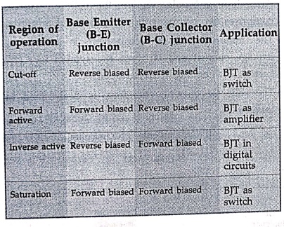
Table 4.3.1 Operating
regions and bias conditions
Inverse Active Mode
•
The active mode of transistor is further classified as forward active and
inverse active.
•
In inverse active mode, B‒E junction (JBE) is reverse biased and B‒C
junction (JBC) is forward bias.
•
In this operating mode, the transistor is operating upside down; that is, the
emitter is acting as the collector and the collector is operating as the
emitter.
•
Fig. 4.3.3 shows the bias conditions for four modes of operations of an npn
transistor.
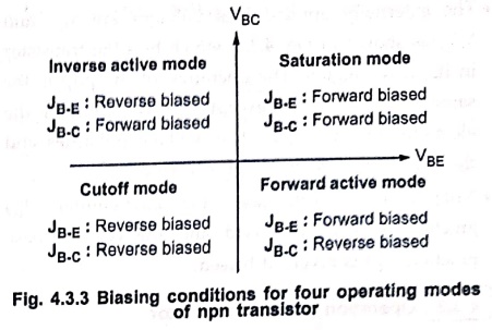
Fig. 4.3.3 Biasing
conditions for four operating modes of npn transistor
•
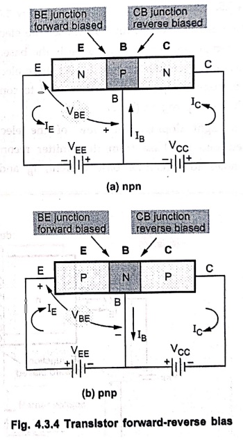
To bias the transistor in its active region, the emitter is base junction
forward biased, while the collector‒base junction in reverse‒biased as shown in
Fig:4.3.4.
•
Fig. 4.3.4 shows the circuit connections for active npn region for both and pnp
transistors.
•
The externally applied bias voltages are VEE and VCC, as
shown in Fig. 4.3.4, which bias the transistor in its active region. The
operation of the pnp is the same as for the npn except that the roles of the
electrons and holes, the bias voltage polarities and the current directions are
all reversed.
•
Note that in both cases the base‒emitter (JE) junction is forward
biased and the collector‒base junction (JC) is reversed biased.
3. Operation of npn Transistor
•
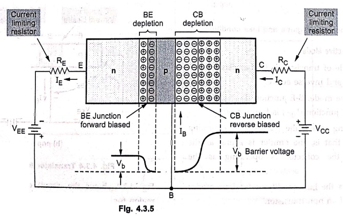
The base to emitter junction is forward biased by the d.c. source VEE.
Thus, the depletion region at this junction is reduced. The collector to base
junction is reverse biased, increasing depletion region at collector to base
junction as shown in Fig. 4.3.5.
•
The forward biased EB junction causes the electrons in the n‒type emitter to
flow towards the base. This constitutes the emitter current IE. As
these electrons flow through the p‒type base, they tend to combine with holes
in p‒region (base).
• Due to light doping, very few of the electrons injected into the base from the emitter recombine with holes to constitute base current, IB and the remaining large number of electrons cross the base region and move through the collector region to the positive terminal of the external d.c. source.
•
This constitutes collector current IC. Thus the electron flow
constitutes the dominant current in an npn transistor.
•
Since, the most of the electrons from emitter flow in the collector circuit and
very few combine with holes in the base. Thus, the collector current is larger
than the base current. The relationship between these current is given by
IE = IC + IB
•
This relationship is also obtained by applying Kirchhoff's current law to the
transistor of Fig. 4.3.4.
•
Since it is a bipolar device, the collector current comprises two components:
Majority and minority.
•
The minority current component is called the leakage current and is given the
symbol Ico (Ic current with emitter terminal open).
•
The collector current, therefore, is determined in total by
IC = ICmajority +ICO
minority
= IC(INJ) + ICO
IC(INT): It is an injected
collector current due to majority carriers crossing the collector base
junction.
4. Operation of pnp Transistor
•
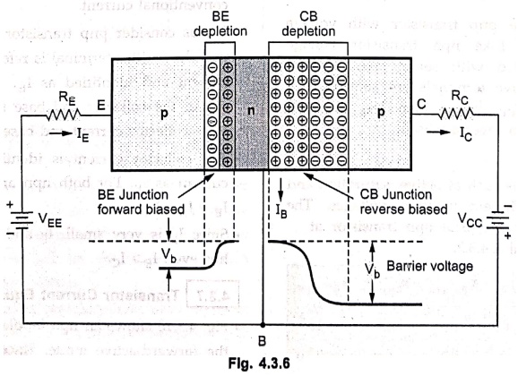
The pnp transistor has its bias voltages VEE and VCC
reversed from those in the npn transistor. This is necessary to forward‒bias
the emitter‒base junction and reverse‒bias the collector base junction.
•
The forward biased EB junction causes the holes in the p‒type emitter to flow
towards the base. This constitutes the emitter current IE.
•
As these holes flow through the n‒type base, they tend to combine with
electrons in n‒region (base). As the base is very thin and lightly doped, very
few of the holes injected into the base from the emitter recombine with
electrons to constitute base current, IB.
• The remaining large number of holes cross the depletion region and move through the collector region to the negative terminal of the external d.c. source. This constitutes collector current IC. Thus the hole flow constitutes the dominant current in an pnp transistor.
5. Transistor Voltages
npn Transistor
•
Fig. 4.3.7 shows the terminal voltages and its polarities for an npn
transistor. The voltage between base and emitter is denoted as VBE.
For VBE, base is positive than emitter because for npn transistor, the
base is biased positive with respect to the emitter.
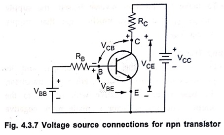
Fig. 4.3.7 Voltage source connections for npn
transistor
• The voltage between the collector and the emitter is denoted as VCE and the voltage between the collector and the base is denoted as VCB. Since collector is positive with respect to base and emitter the polarities are as shown in Fig. 4.3.7.
•
Fig. 4.3.7 shows the npn transistor with voltage connections. The voltage
sources are connected to the transistor with series resistors. These resistors
are called current limiting resistors.
•
The base supply voltage VBB is connected via resistor RB,
and the collector supply voltage, VCC is connected via resistor RC.
•
The negative terminals of both the supply voltages are connected to emitter
terminal of the transistor.
•
To make CB junction reverse biased, the supply voltage VCC is always
much larger than supply voltage VBB.
pnp Transistor
•
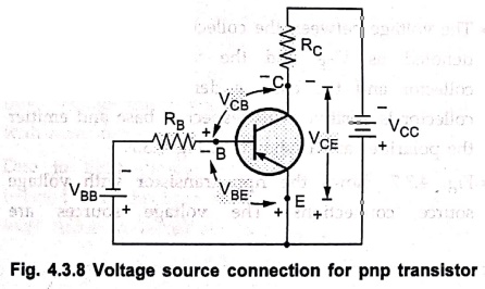
Fig. 4.3.8 shows the terminal voltages and its polarities for a pnp transistor.
For a pnp transistor, the base is biased negative with respect to the emitter,
and the collector is made more negative than the base.
•
Fig. 4.3.8 shows the pnp transistor with voltage source connections. Like npn
transistor voltage sources are connected with series resistors. The source
voltage positive terminals are connected at the emitter with VCC
larger than VBB to keep collector‒base junction reverse biased.
Junction Voltages
•
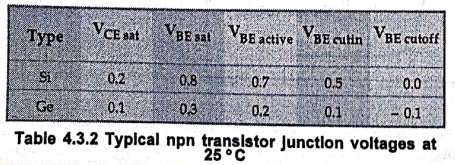
In different conditions such as active, saturation and cutoff there are
different junction voltages. The junction voltages for a typical npn transistor
at 25 °C are given in Table 4.3.2.
•
The entries in the table are appropriate for an npn transistor. For pnp
transistor the signs of all entries should be reversed.
6. Transistor Currents
•
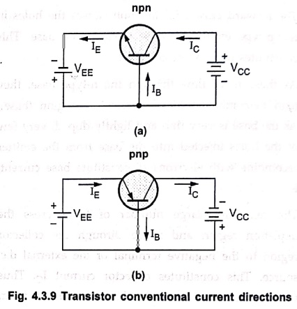
The directions of conventional currents in an npn transistor are as shown in
Fig. 4.3.9 (a) and those for a pnp are shown in Fig. 4.3.9 (b).
•
It can be noticed that the arrow at the emitter of the transistor's symbol
points in the direction of conventional current.
•
Let us consider pnp transistor. The current flowing into the emitter terminal
is referred to as the emitter current and identified as IE. The
currents flowing out of the collector and base terminals are referred to as
collector current and base current, respectively.
•
The collector current is identified as IC and base current as IB.
For both npn and pnp transistors,
IE = IB + IC.
•
Since IB is very small, IE and IC are nearly
equal; however, IE > IC.
7. Transistor Current Equations
•
Fig. 4.3.10 shows an npn bipolar transistor biased in the forward‒active mode.
Since the B‒E junction is forward biased, electrons from the emitter are injected
across the B‒E junction into the base, creating an excess minority carrier
concentration in the base.
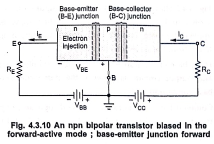
Fig. 4.3.10 An npn
bipolar transistor blased In the forward‒active mode; base‒emitter junction
forward
•
The base region is very narrow so that, in the ideal case, the injected
electrons will not recombine with any of the majority carrier holes in the
base. In this case, the minority carrier electron concentration in the base is
a linear function of distance as shown in Fig. 4.3.11.
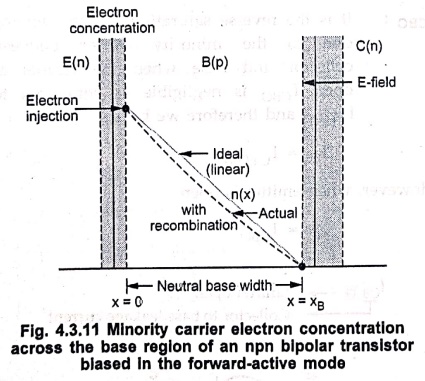
Fig. 4.3.11 Minority
carrier electron concentration across the base region of an npn bipolar
transistor blased in the forward‒active mode
•
The electrons that are injected from the emitter region diffuse across the
base, are swept across the base‒collector space‒charge region by the electric
field, and are collected in the collector region creating the collector
current.
•
However, some carrier recombination does occur in the base. In this case, the
electron concentration will deviate from the ideal linear curve, as shown in
Fig. 4.3.11.
•
To minimize recombination effects, the width of the neutral base region is kept
small compared to the minority carrier diffusion length.
•
Emitter current: Since the B‒E junction is forward biased, the current through
this junction is an exponential function of B‒E voltage. Thus, we can write the
current at the emitter terminal as
IE = ISE exp (VBE
/VT)
•
VT is the usual thermal voltage. The multiplying constant, ISE,
contains electrical parameters of the junction. It is directly proportional to
the active B‒E cross sectional area.
•
Collector current: It is proportional to the emitter current and is given by
IC = αF IE =
αF ISE еvBE/VT
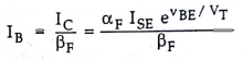
•
Base current: It is given as
IB = IC/BF =
[ αF ISE еvBE/VT ] / βF
Review
Questions
1. Explain various voltage components of transistor.
2. Explain the various current components of the transistor.
3. Write equations for collector current (IC) in
terms of emitter current (IE) and αdc, and in terms of
base current (IB) and αdc.
4. Draw a sketch to show the various current components in a NPN
transistor and deduce the relation between various current components.
5. Sketch the symbols of transistors and mark the current
directions.
6. Give the biasing arrangement for an NPN transistor to operate
in the active region.
7. Sketch and explain the minority carrier electron
concentration across the base region of an npn bipolar transistor biased in the
forward‒active mode.
8. State expressions of IC, IE and IB.
9. What is the need for biasing in the transistor?
10. Describe the working of PNP transistor.
Electron Devices: Chapter 4: Bipolar Junction Transistors : Tag: electronics : - Principle of Operation of Bipolar Junction Transistors (BJT)
Electron Devices: Chapter 4: Bipolar Junction Transistors
Under Subject

Electron Devices
EC25C01 2nd Semester ECE Dept | 2025 Regulation | 2nd Semester 2025 Regulation
Related Subjects

English Essentials II
EN25C02 2nd Semester | 2025 Regulation | 2nd Semester 2025 Regulation

Tamils and Technology தமிழர்களும் தொழில்நுட்பமும்
UC25H02 2nd Semester | 2025 Regulation | 2nd Semester 2025 Regulation

Linear Algebra
MA25C02 2nd Semester | 2025 Regulation
Electron Devices
EC25C01 2nd Semester ECE Dept | 2025 Regulation | 2nd Semester 2025 Regulation

Data Structures using CPlusPlus
CS25C05 2nd Semester ECE Dept | 2025 Regulation | 2nd Semester 2025 Regulation

Circuits and Network Analysis
EC25C02 2nd Semester ECE Dept | 2025 Regulation | 2nd Semester 2025 Regulation

Re-Engineering for Innovation
ME25C05 2nd Semester | 2025 Regulation | 2nd Semester 2025 Regulation

Engineering Drawing - Laboratory
ME25C01 2nd Semester | 2025 Regulation | 2nd Semester 2025 Regulation

Data Structures using CPlusPlus - Laboratory
CS25C05 2nd Semester ECE Dept | 2025 Regulation | 2nd Semester 2025 Regulation

Devices and Circuits Laboratory
EC25C03 2nd Semester ECE Dept | 2025 Regulation | 2nd Semester 2025 Regulation