Computer Organization and Architecture: Chapter 3: Processor Design
Processor Design: Important Example Solved Problems
Computer Organization and Architecture
Computer Organization and Architecture: Chapter 3: Processor Design: Anna University Solved Problems, Assignment Problems and Important Solved Problems
Hardwired Control
Example: 1
Generate the logic circuit for the following function
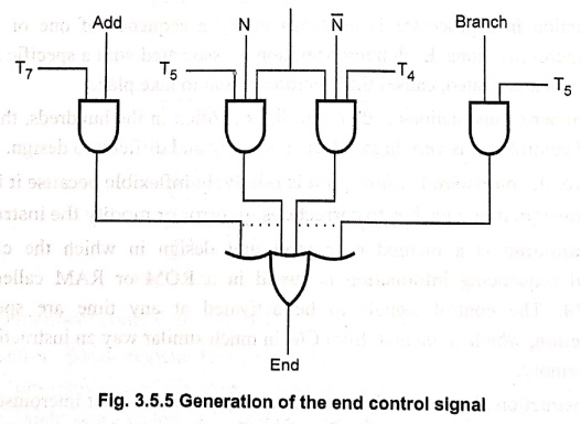
End = T7 .ADD +T5 BR + (T5 . N + T4 .  ) BRN + ….
Solution:
Fig. 3.5.5 shows the circuit that generates the End control signal from the logic function.
End = T7 . ADD + T5 . BR + (T5 . N + T4) . BRN + ......
Microprogrammed Control
Example: 1
Write a combined micro routine that can implement that BGT (Branch if > 0), BPL (Branch if plus) and BR (Branch Unconditionally) instructions. The branch conditions. for the BGT and BPL instructions are Z + (N XOR V) = 0 and N = 0, respectively. What is the total number of micro instructions required? How many micro instructions are needed if a separate micro routine is used for each machine instruction?
Solution:
For bus organisation, we write microroutine for the implementation of BGT (Branch if > 0), BPL (Branch if plus) and BR (Branch unconditionally) instructions as follows.
Combine Microroutine
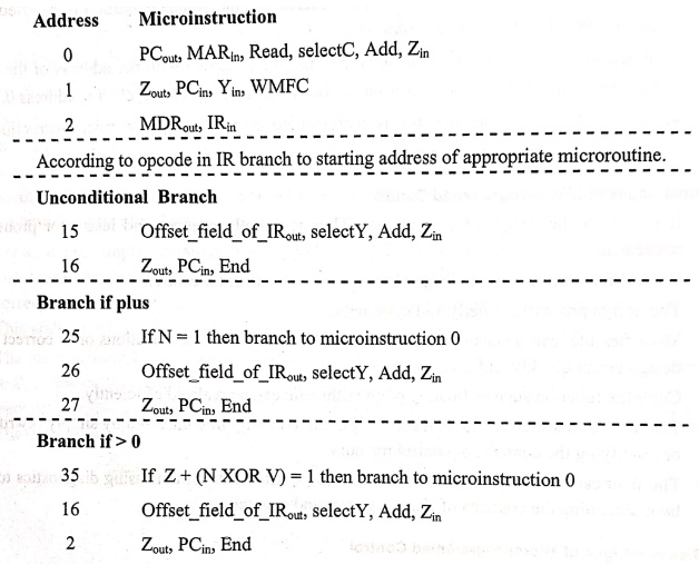
• The first three microinstructions in the combine microroutine are used to fetch the opcode. The total number of microinstructions required are 11. If a separate microroutine is used for el each machine instruction 17 microinstructions are needed.
Example: 2
For a single bus organisation of CPU, write a microprogram for instruction. Add (Rsrc) +,R dst.
Solution:
Let us examine the path needed for the flowchart in 3.6.5 to execute the instruction Add(Rsrc)+, Rdst
In this instruction the source operand is accessed in the autoincrement mode and the Rsrc and Rast are general purpose registers in the processor. We assume that the processor has 16 registers that can be used for addressing purpose, each specified using a 4‒bit code. We also assume that the instruction has a 3‒bit field, (bits 8‒10) used to specify the addressing mode for the source operand, as shown in Fig. 3.6.6. Bit patterns 11,10,01 and 00 located in bits 10 and 9 denote the indexed, auto decrement, autoincrement and register modes respectively. For each of these modes bit‒8 is used to specify the indirect version. For example, 100 in the mode field specifies the direct version of the autodecrement mode, whereas 101 specifies the indirect version.
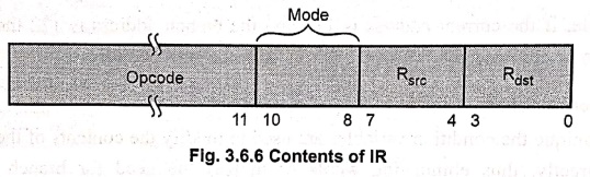
As a part of execution, first the opcode and mode fields are decoded to determine that an Rsrc or Rdst register is involved. The decoded output is then used to gate the contents of the Rsrc or Rdst fields in the IR into a second decoder, which produces the gating signals for the actual registers R0 to R15.
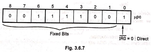
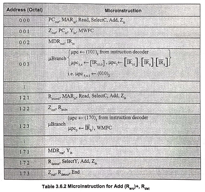
The flowchart of a microprogram for the ADD Rsrc, Rdst instruction in Fig. 3.6.5 is drawn by combining the microroutines for all possible values of the mode field, resulting in a structure that requires many branch points. The instruction Add (Rsrc)+, Rdst requires two branch microinstructions. In each branch microinstruction, the expression in brackets indicates the branch address that is to be loaded into the upc and how this address is modified using the bit‒ORing scheme. For example, the branch instruction at location 123 modifies the branch address 170 to 171 by ORing the bit‒8 in the IR with bit pc0 to change the addressing mode from indirect to direct, as shown in Fig. 3.6.7.
The address for branch microinstruction at location 003 is generated as shown in Fig. 3.6.8.
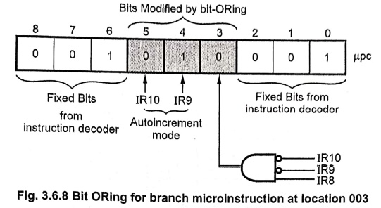
Table 3.6.2 gives the microinstruction sequence for the execution of Add (Rsrc)+, Rdst instruction.
Example: 3
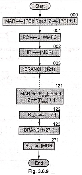
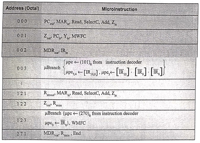
For a single bus organisation of data paths inside the CPU, write a microprogram of micro‒instructions and draw chart of a microprogram for the following instruction.MOV (Rsrc)+, Rdst
Rast uses direct and autoincrement addressing.
Solution: Flowchart
Basic Concepts of Pipelining
Example: 1
Explain the function of a six segment pipeline and draw a space diagram for a six segment pipeline showing the time it takes to process eight tasks.
Solution: Six stages in the pipeline :
1) Fetch Instruction (FI) : Read the next expected instruction into a buffer.
2) Decode Instruction (DI) : Determine the opcode and the operand specifiers.
3) Calculate Operands (CO) : Calculate the effective address of each source operand.
4) Fetch Operands (FO) : Fetch each operand from memory.
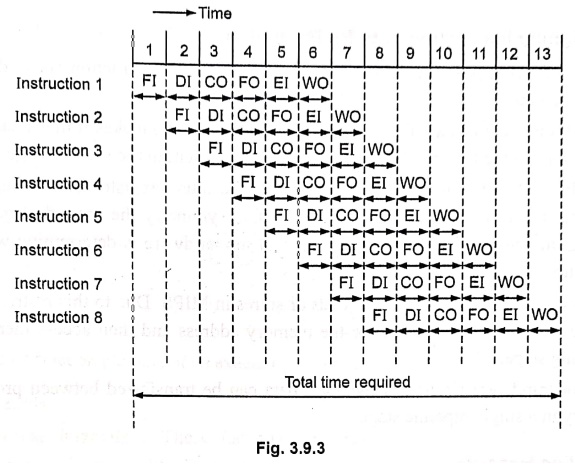
5) Execute Instruction (EI) : Perform the indicated operation and store the result, if any in the specified destination operand location.
6) Write Operand (WO) : Store the result in memory.
Example: 2
What is the ideal speed‒up expected in a pipelined architecture with 'n' stages? Justify your answer.
Solution:
The pipelined processor ideally completes the processing of one instruction in each clock cycle, which means that the rate of instruction processing with n stage pipeline is n times that of sequential operation. Therefore, ideal speed‒up factor is n. However, such ideal performance of the pipeline is achieved only when pipeline stages must complete their processing tasks for a given instruction in the time allotted. Unfortunately, this is not the case; pipeline operations could not sustained without interruption throughout the program execution.
Handling Data Hazards
Example: 1
Convert the following code segment in C to MIPS instructions, assuming all variables are in memory and are addressable as offsets from $t0 :
a = b+e ;
c = b+f ;
Solution :
lw $t1, 0($t0)
lw $t2, 4($t0)
add $t3, $t1,$t2
sw $t3, 12($t0)
lw $t4, 8($t0)
add $t5, $t1,$t4
sw $t5, 16($t0)
Example: 2
Find the hazards in the code segment of the previous example and reorder the instructions to avoid any pipeline stalls.
Solution:
Both add instructions have a hazard because of their respective dependence on the immediately preceding lw instruction. It is important to note that bypassing eliminates several other potential hazards, including the dependence of the first add on the first lw and any hazards for store instructions. Moving up the third lw instruction to become the third instruction eliminates both hazards:
lw $t1, 0($t0)
lw $t2, 4($t0)
lw $t4, 8($t0)
add $t3, $t1,$t2
sw $t3, 12($t0)
add $t5, $t1,$t4
sw $t5, 16($t0)
Example: 3
The following sequence of instructions are executed in the basic 5 ‒ stage pipelined processor.
or rl, r2, r3
or r2, rl, r4
or rl, rl, r2
a) Indicate dependences and their type.
b) Assume there is no forwarding in this pipelined processor. Indicate hazards and add NOP instructions to eliminate them.
c) Assume there is full forwarding. Indicate hazards and add NOP instructions to eliminate them.
Solution:
a) Dependences and their type
• Read After Write (RAW) dependency in rl between Instructions 1, 2 and 3.
• Read After Write (RAW) dependency in r2 between Instructions 2 and 3.
• Write After Read (WAR) in r2 from Instruction 1 to 2.
• Write After Read (WAR) in rl from Instruction 2 to 3.
• Write After Read (WAR) in rl from Instruction 1 to 3.
b) No hazards from write after read and write after write, since there are 5 stages. Read after writes cause data hazards.
or rl, r2, r3
NOP
NOP
or r2, r1, r4
NOP
NOP
or rl, rl, r2
c) In full forwarding the data hazards above are eliminated, thus there is no need for NOP instructions.
Handling Control Hazards
Example: 1
The following sequence of instructions are executed in the basic 5‒stage pipelined processor :
lw$1, 40($6)
add $6, $2, $2
sw $6, 50($1)
Indicate dependence and their type. Assuming there is no forwarding in this pipelined processor, indicate hazards and add NOP instructions to eliminate them.
Solution:
a) I1: 1w $1, 40($6): Raw dependency on $1 from I1 to I3
I2: add $6, $2, $2: Raw dependency on $6 from I2 to I3
I3: sw $6,50 ($1) : WAR dependancy on $6 from I1 to I2 and I3
b) In the basic five‒stage pipeline WAR dependency does not cause any hazards. Assuming there is no forwarding in this pipelined processor RAW dependencies cause hazards – if register read happens in the second half of the clock cycle and the register write happens in the first half. The code that eliminates these hazards by inserting nop instruction is:
1w $1, 40($6)
add $6, $2, $2
nop; delay 13 to avoid RAW hazard on $1 from I1
sw $6,50($1)
Example: 2
A processor has five individual stages, namely, IF, ID, EX, MEM and WB and their latencies are 250 ps, 350 ps, 150 ps, 300 ps, and 200 ps respectively. The frequency of the instructions executed by the processor are as follows; ALU: 40%, Branch 25 % load: 20% and store 15%. What is the clock cycle time in a pipelined and non‒pipelined processor? If you can split one stage of the pipelined datapath into two new stages, each with half the latency of the original stage, which stage would you split and what is the new clock cycle time of the processor? Assuming there are no stalls or hazards, what is the utilization of the data memory? Assuming there are no stalls or hazards, what is the utilization of the write register port of the "Registers" unit?
Solution:
a) Clock cycle time in a pipelined processor = 350 ps
Clock cycle time in non‒pipelined processor
= 250 ps + 350 ps + 150 ps + 300 ps + 200 ps = 1250 ps
b) We have to split one stage of the pipelined datapath which has a maximum latency
i.e. ID.
After splitting ID stage with latencies ID1 = 175 ps and ID2 = 175 ps we have new clock cycle time of the processor equal to 300 ps
c) Assuming there are no stalls or hazards, the utilization of the data memory
= 20% to 15% = 35 %
d) Assuming there are no stalls or hazards, the utilization of the write ‒ register port of the register unit = 40% +25% = 65%
Computer Organization and Architecture: Chapter 3: Processor Design : Tag: Computer : Computer Organization and Architecture - Processor Design: Important Example Solved Problems
Computer Organization and Architecture: Chapter 3: Processor Design
Under Subject
Computer Organization and Architecture
CW25201 3rd Semester IT department. | 2025 Regulation | 3rd Semester 2025 Regulation
Related Subjects
Discrete Mathematics
MA25C14 3rd Semester CSE,IT,CY,AIDS departments. | 2025 Regulation | 3rd Semester 2025 Regulation
Data Structures
CS25C08 3rd Semester CSE,IT,CY,AIDS departments. | 2025 Regulation | 3rd Semester 2025 Regulation
Computer Organization and Architecture
CW25201 3rd Semester IT department. | 2025 Regulation | 3rd Semester 2025 Regulation
Object Oriented Programming
CS25C07 3rd Semester IT department. | 2025 Regulation | 3rd Semester 2025 Regulation
Web Technologies
IT25301 3rd Semester IT department. | 2025 Regulation | 3rd Semester 2025 Regulation
English Communication Skills Laboratory I
EN25C03 3rd Semester all department. | 2025 Regulation | 3rd Semester 2025 Regulation
Skill Development Course I
3rd Semester all department. | 2025 Regulation | 3rd Semester 2025 Regulation