Computer Organization and Architecture: Chapter 3: Processor Design
Implementation of Basic MIPS ISA
Processor Design

Questions: 1. Draw and explain the functional block diagram for implementation of MIPS subset. 2. Draw and explain the function block diagram with control signals for basic implementation of MIPS subset. 3. Explain the basic MIPS implementation with necessary multiplexers and control lines. 4. Write the two steps that are common to implement any type of instruction.
Computer
Organization and Architecture
Chapter 3:
Processor
Design
Implementation
of Basic MIPS ISA
•
In this chapter we will see the implementation of a subset of the core MIPS
instruction set.
These
instructions are divided into three classes :
■
The memory‒reference instructions: load
word (lw) and store word (sw)
■
The arithmetic‒logical instructions: add,
sub, AND, OR and slt
■
The branch instructions: branch equal
(beq) and jump (j)
•
The subset considered here does not include all the integer instructions (for
example, shift, multiply and divide are missing), nor does it include any
floating‒point instructions. The key principles used in creating a datapath and
designing the control are discussed here. The implementation of the remaining
instructions is somewhat similar.
•
For implementing every instruction, the first two steps are same :
1. Fetch the
instruction: Send the Program Counter (PC) contents
(address of instruction) to the memory that contains the opcode and fetch the
instruction from that memory.
2. Fetch operand(s) :
Read one or two registers, using fields of the instruction to select the
registers to read. For the load word instruction, we need to read only one
register, but most other instructions we require to read two registers.
•
The remaining actions required to complete the instruction depend on the
instruction class. For each of the three instruction classes (memory‒reference,
arithmetic‒logical and branches), the actions are mostly the same, independent
of the exact instruction. This shows that the simplicity and regularity of the MIPS instruction set simplifies
the implementation by making the execution of many of the instruction classes
similar.
•
For example, all instruction classes, except jump, use the Arithmetic‒Logical
Unit (ALU) after reading the registers.
■
Memory‒reference instructions use the ALU for an address calculation.
■
Arithmetic‒logical instructions use the ALU for the operation execution and
■
Branches use the ALU for comparison.
•
After using the ALU, the actions required to complete various instruction
classes are not same.
■
A memory‒reference instruction needs to access the memory either to read data
for a load or write data for a store.
■
An arithmetic‒logical or load instruction must write the data from the ALU or
memory back into a register.
■
A branch instruction may need to change the next instruction address based on
the comparison; otherwise, the PC should be incremented by 4 to get the address
of the next instruction.
•
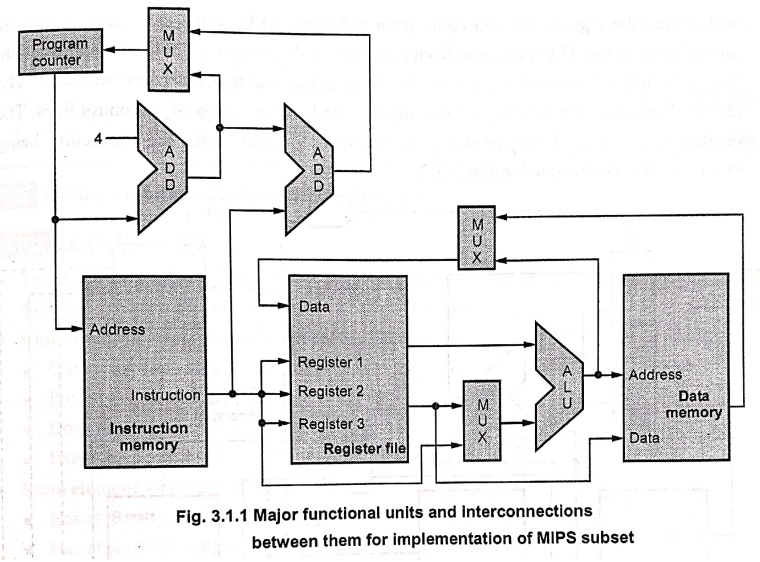
Fig. 3.1.1 shows the block diagram of a MIPS implementation, showing the
functional units and interconnection between them.
Operation
•
The program counter gives the instruction address to the instruction memory.
•
After the instruction is fetched, the register operands required by an
instruction are specified by fields of that instruction.
•
Once the register operands have been fetched, they can be used to compute a
memory address (for a load or store), to compute an arithmetic result (for an integer
arithmetic‒ logical instruction) or a compare (for a branch).
•
If the instruction is an arithmetic‒logical instruction, the result from the
ALU must be written to a register.
•
If the operation is a load or store, the ALU result is used as an address to
either store a value from the registers or load a value from memory into the
registers. The result from the ALU or memory is written back into the register
file.
•
Branches require the use of the ALU output to determine the next instruction
address, which comes either from the ALU (where the PC and branch offset are
summed) or from an adder that increments the current PC by 4.
•
Fig. 3.1.1 shows that data going to a particular unit is coming from two
different sources. For example, the value written into the PC can come from one
of two adders, the data written into the register file can come from either the
ALU or the data memory and the second input to the ALU can come from a register
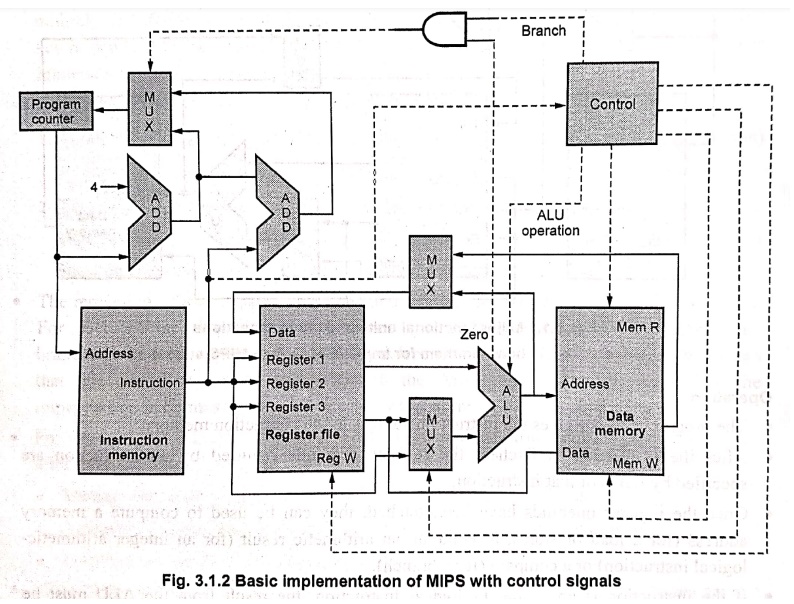
or the immediate field of the instruction. The selection of appropriate source
is done using multiplexer (data selector). The multiplexer selects from among
several inputs based on the setting of its control lines. The control lines are
set based primarily on information taken from the instruction being executed.
This is illustrated in Fig. 3.1.2.
•
Fig. 3.1.2 also shows the control unit, which has the instruction as an input,
is used to determine the control signals for the functional units and two of
the multiplexers.
•
The third multiplexer, which determines whether PC + 4 or the branch
destination address is written into the PC, is set based on the Zero output of the ALU, which is used
to perform the comparison of a beq
instruction.
Review Questions
1. Draw and explain
the functional block diagram for implementation of MIPS subset.
2. Draw and explain
the function block diagram with control signals for basic implementation of MIPS
subset.
3. Explain the basic
MIPS implementation with necessary multiplexers and control lines.
4. Write the two steps
that are common to implement any type of instruction.
Computer Organization and Architecture: Chapter 3: Processor Design : Tag: Computer : Processor Design - Implementation of Basic MIPS ISA
Computer Organization and Architecture: Chapter 3: Processor Design
Under Subject
Computer Organization and Architecture
CW25201 3rd Semester IT department. | 2025 Regulation | 3rd Semester 2025 Regulation
Related Subjects
Discrete Mathematics
MA25C14 3rd Semester CSE,IT,CY,AIDS departments. | 2025 Regulation | 3rd Semester 2025 Regulation
Data Structures
CS25C08 3rd Semester CSE,IT,CY,AIDS departments. | 2025 Regulation | 3rd Semester 2025 Regulation
Computer Organization and Architecture
CW25201 3rd Semester IT department. | 2025 Regulation | 3rd Semester 2025 Regulation
Object Oriented Programming
CS25C07 3rd Semester IT department. | 2025 Regulation | 3rd Semester 2025 Regulation
Web Technologies
IT25301 3rd Semester IT department. | 2025 Regulation | 3rd Semester 2025 Regulation
English Communication Skills Laboratory I
EN25C03 3rd Semester all department. | 2025 Regulation | 3rd Semester 2025 Regulation
Skill Development Course I
3rd Semester all department. | 2025 Regulation | 3rd Semester 2025 Regulation